| Research |
| Transistor laser |
|
|
| Ⅰ.Transistor
laser |
|
|
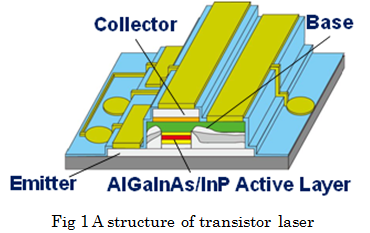
We propose a new light source “Transistor
Laser (TL)” for next generation optical
communication. The structure of a TL (Fig. 1) is
similar to that of n-p-n hetero-junction bipolar
transistor (HBT). Electrons injected from an
emitter are diffused, and a portion of the
electrons is recombined at the active layer while
the rest are removed from the collector. Due to
this carrier pulling effect, fast carrier supply
to the active layer is realized and as a result,
high-speed modulation beyond conventional laser
diodes can be achieved.
We adopt AlGaInAs/InP active layer. With this
alloy, a large gain and superior thermal
characteristics are obtained. The structure of a
TL is based on buried-heterostructure (BH) to
achieve high performance. |
|
|
|
| Ⅱ.Experimental
results |
|
|
|
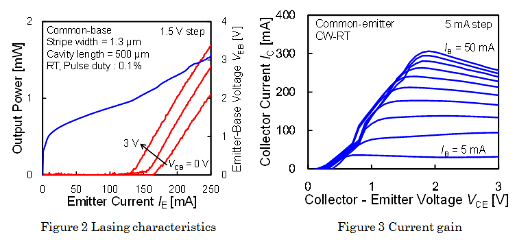
Figure 2 shows lasing characteristics under
common-base configuration. First lasing
operation under room-temperature pulse
condition was achieved. The threshold current
was 160 mA and the external quantum efficiency
from both facets was 2.5%. Figure 3 shows
current characteristics of the device. Current
gain 6~8 was obtained. As the graph shows,
lasing and transistor operation were
demonstrated.
|
|
|
|
|
|
|
| List of reports |
| Journal Papers |
|
(1) M. Shirao, S. Lee, N. Nishiyama, and S.
Arai, “Large-signal Analysis of a Transistor
Laser”, IEEE J. Quantum Electron, Vol. 47, No.
3, pp. 359-367, Mar. 2011.
(2) M. Shirao, T. Sato, Y. Takino, N. Sato, N.
Nishiyama, and S. Arai, “Room-Temperature
Continuous-Wave Operation of 1.3-μm Transistor
Laser with AlGaInAs/InP Quantum Wells”, Appl.
Phys. Express, Vol. 4, No. 7, pp. 072101-1-3,
June 2011.
(3) Y. Takino, M. Shirao, T. Sato, N.
Nishiyama, T. Amemiya, and S. Arai, “Regrowth
Interface Quality Dependence on Thermal
Cleaning of AlGaInAs/InP Buried-Heterostructure
Lasers”, Jpn. J. Appl. Phys., Vol. 50, No. 7,
pp. 070203-1-070203-3, July 2011.
(4) M. Shirao, T. Sato, N. Sato, N. Nishiyama,
and S. Arai, “Room-Temperature Operation of
1.3-μm Transistor Laser with AlGaInAs/InP
Quantum Wells”, Opt. Express, Vol. 20, No. 4,
pp. 3983-3989, Feb. 2011.
5) Y. Takino, M. Shirao, N. Sato, T. Sato, N.
Nishiyama, T. Amemiya, and S. Arai, “Improved
Regrowth Interface of
AlGaInAs/InP-Buried-Heterostructure Lasers by
In-Situ Thermal Cleaning”, J. Quantum.
Electron., Vol. 48, No. 8, pp. 971-979, Aug.
2012.
|
| |
| International
Conferences |
|
(1) M. Shirao, N. Nishiyama, S. Lee, and S.
Arai, “Large Signal Analysis of AlGaInAs/InP
Laser Transistor”, Conference on Lasers and
Electro Optics/International Quantum
Electronics conference (CLEO/IQEC 2010), CMY 7,
May 2010.
(2) Y. Takino, M. Shirao, T. Sato, N.
Nishiyama, and S. Arai, “Investigation of
Regrowth Interface Quality of AlGaInAs/InP
Buried Heterostructure Lasers”, The 22nd
International Conference on Indium Phosphide
and Related Materials (IPRM 2010), Wep27, May
2010.
(3) M. Shirao, T. Sato, Y. Takino, N. Sato, N.
Nishiyama, and S. Arai, “Lasing Operation of
Long-Wavelength Transistor Laser Using
AlGaInAs/InP Quantum Well Active Region”, The
23rd International Conference on Indium
Phosphide and Related Materials (IPRM 2011),
Tu-3.2.4, May 2011.
(4) N. Sato, Y. Takino, M. Shirao, T. Sato, N.
Nishiyama, and S. Arai, “Effect of Thermal
Cleaning on Regrowth Interface Quality of
AlGaInAs/InP Buried Heterostructure Lasers”,
The 38th International Symposium on Compound
Semiconductors (ISCS 2011), P5.60, May
2011.
(5) T. Sato, M. Shirao, N. Sato, N. Nishiyama,
and S. Arai, “Room-Temperature Lasing Operation
of a 1.3-μm npn-AlGaInAs/InP Transistor Laser”,
The IEEE Photonic 2011 Conference (IPC 2011),
WDD5, Oct. 2011.
(6) N. Sato, M. Shirao, T. Sato, M. Yukinari,
N. Nishiyama, T. Amemiya, and S. Arai,
“Room-Temperature Continuous-Wave Operation of
a 1.3-μm npn-AlGaInAs/InP Transistor Laser”,
The 23rd IEEE International Semiconductor Laser
Conference (ISLC 2012), MA7, Oct. 2012.
|
| |
| Domestic Conferences |
|
(1) M. Shirao, D. Imanishi, N. Nishiyama,
and S. Arai, “長波長帯レーザトランジスタ実現へ向けたベース層の構造設計”,
The 69th Autumn Meeting; The Japan Society of
Applied Physics, 2p-P3-7, Sep. 2008.
(2) M. Shirao, Y. Takino, S. Lee, N. Nishiyama,
and S. Arai,
“レート方程式によるAlGaInAs長波長帯レーザトランジスタの動作解析”, The 70th
Autumn Meeting; The Japan Society of Applied
Physics, Digest III, 10p-S-10, Sep. 2009.
(3) M. Shirao, N. Nishiyama, S. Lee, and S.
Arai,
“AlGaInAs量子井戸活性層を有する長波長帯レーザトランジスタ変調効率の構造依存性”,
The 57th Spring Meeting; The Japan Society of
Applied Physics, 19p-E-6, Mar. 2010.
(4) Y. Takino, M. Shirao, T. Sato, N.
Nishiyama, and S. Arai,
“AlGaInAs/InP埋め込みヘテロ構造レーザにおける再成長界面品質のサーマルクリーニング依存性”,
The 57th Spring Meeting; The Japan Society of
Applied Physics, 19p-E-4, Mar. 2010.
(5) Y. Takino, M. Shirao, T. Sato, N.
Nishiyama, and S. Arai,
“AlGaInAs埋め込みヘテロ構造レーザにおけるサーマルクリーニング中雰囲気の再成長界面品質に対する影響”,
The 71st Autumn Meeting; The Japan Society of
Applied Physics, 19p-H-14, Aug. 2010.
(6) M. Shirao, N. Nishiyama, S. Lee, and S.
Arai, “3端子を有するヘテロ接合バイポーラトランジスタ型SOAの数値解析”, The
58th Spring Meeting; The Japan Society of
Applied Physics, 27a-P8-10, Mar. 2011
(7) T. Sato, M. Shirao, Y. Takino, N.
Nishiyama, and S. Arai,
“1.3-μm帯pnp-AlGaInAsレーザトランジスタの室温連続動作”, The 58th
Spring Meeting; The Japan Society of Applied
Physics, 26a-P5-14, Mar. 2011.
(8) N. Sato, Y. Takino, T. Sato, M. Shirao, N.
Nishiyama, and S. Arai,
“AlGaInAs/InP埋め込みヘテロ構造レーザにおけるサーマルクリーニング中温度の再成長界面品質に対する影響”,
The 58th Spring Meeting; The Japan Society of
Applied Physics, 26a-P5-15, Mar. 2011.
(9) T. Sato, M. Shirao, N. Sato, N. Nishiyama,
and S. Arai,
“1.3-μm帯npn-AlGaInAsレーザトランジスタの室温パルス動作”, The
72nd Autumn Meeting; The Japan Society of
Applied Physics, 1a-ZL-10, Sep. 2011.
(10) N. Sato, M. Shirao, T. Sato, N. Nishiyama,
and S. Arai,
“ICP-RIEを用いたAlGaInAs/InP埋め込みヘテロ構造レーザ”, The 72nd
Autumn Meeting; The Japan Society of Applied
Physics, 1a-ZL-9, Sep. 2011.
(11) Sato, M. Shirao, N. Sato, M. Yukinari, N.
Nishiyama, and S. Arai,
“1.3-μm帯npn-AlGaInAsレーザトランジスタの室温連続動作”, The 59th
Spring Meeting; The Japan Society of Applied
Physics, 16a-F3-8, Mar. 2012.
|
|
|
| △ Top to the
page △ |
|