| |
| 研究内容 |
| Hybrid integrated III-V semiconductor lasers on Silicon on Insulator (SOI) |
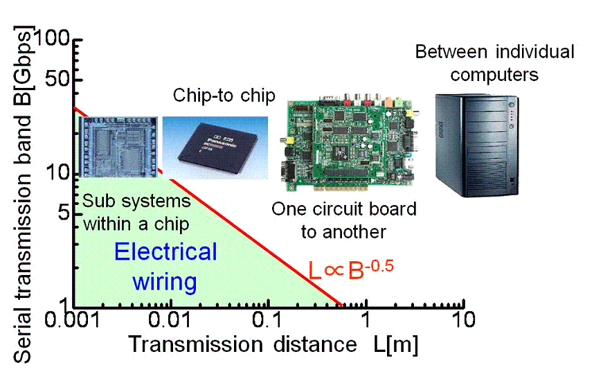
Electronics technologies such as CMOS-LSI have been developed with a scaling.
But it has been predicted that the continuing growth of silicon LSI technology will soon hit a bottleneck due to ohmic heating and RC delay caused by metal lines.
One of the promising solutions is optical interconnection, which can be realized by replacing metal lines with optical lines of board to board or chip to chip as shown in fig. 1.
Silicon is suitable for optical-fiber communication due to its transparency at wavelengths above 1.1 μm.
Besides, it can also be used to construct high-index-contrast waveguides between a Si core (n = 3.45) and oxide cladding layers (n = 1.45).
CMOS-based technologies can be applied to Si photonic integrated circuits. Therefore, silicon-on-insulator (SOI) substrates can be used to realize ultracompact photonic circuits.
The only disadvantage is that Si is an indirect transition type semiconductor and not suitable for such active devices.
Optical light sources integrated with Silicon are strongly required for the optical interconnection.
|
|
| Fig.1:Relation between bandwidth and distance |
We are engaged in research for GaInAsP semiconductor membrane DFB laser, which has been studied in our group, on SOI substrate.
For the optical interconnection on Si platform, low power dissipation, device integration and small footprint are required for optical devices.
In addition, it is necessary for semiconductor lasers to have stable single mode operation to achieve wavelength division multiplexing systems
We have reported the several semiconductor laser on SOI by direct bonding technique. |
| |
| |
(1) Light emitting device on Si substrate
Figure 2 shows GaInAsP semiconductor membrane structure and lasing characteristics of membrane BH-DFB laser on SOI substrate. The fine membrane layers with quantum well active layer on 60nm thick SOI layers can be seen. We developed low damage direct wafer bonding technique for membrane based optical device. In addition, room temperature, continuous wave lasing operation of 2.8 mW threshold pump power was obtained.
|
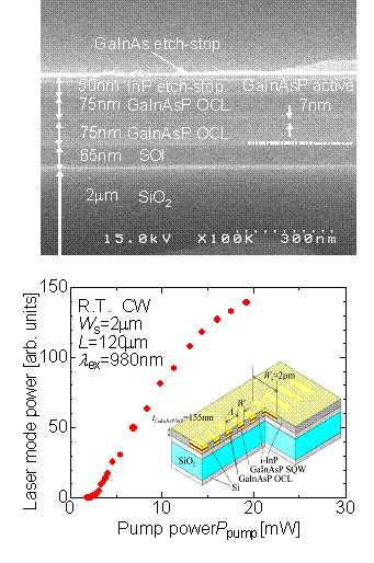 |
Fig. 2: GaInAsP/InP QW structure directly bonded on SOI
and a lasing characteristic of DFB laser
|
|
| |
(2)Waveguide integration
In the optical interconnection, it is important for lasers on SOI to output the light to Si waveguide. We have reported membrane DFB laser integrated with passive Si ridge-waveguide. Then, further research such as high efficient integration between laser and passive waveguide are being carried on toward an optical data transmission on Si-chip
|
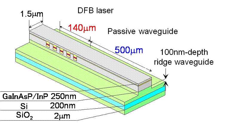 |
| Fig. 3:Membrane DFB laser integrated with Si waveguide |
(3)Injection type laser
For semiconductor lasers on SOI, besides membrane lasers, electrically pumped operation requires much effort because the difference layer structure from conventional double hetero laser. In addition, optical output into the SOI layer should be considered. As a first trial, we succeeded in an injection type DFB laser with wire like active region on SOI substrate and now, try to improve the performance and to realize multifunctional devices.
|
|
| |
| List of reports |
(1) Publication |
- T. Okumura, T. Maruyama, H. Yonezawa, N. Nishiyama, and S. Arai: “Injection-type GaInAsP/InP/Si Distributed-feedback Laser Directly Bonded on Silicon-on-insulator Substrate,” IEEE Photon. Technol. Lett. Vol. 21, No. 5, pp. 283-285, Mar. 2009.
- T. Okumura, T. Maruyama, M. Kanemaru, S. Sakamoto, and S. Arai:“Single-modeoperation of GaInAsP/InP-membrane distributed feedback (DFB) lasers bonded on silicon-on-insulator (SOI) substrate with rib-waveguide structure,” Jpn. J. Appl. Phys., Vol. 46, No. 48, pp. L1206-L1208, Dec. 2007.
- T. Maruyama, T. Okumura, and S. Arai: “Direct wafer bonding of GaInAsP/InP membrane structure on silicon-on-insulator substrate,” Jpn. J. Appl. Phys., Vol. 45, No. 11, pp. L8717-L8718, Nov. 2006.
- T. Maruyama, T. Okumura, S. Sakamoto, K. Miura, Y. Nishimoto, and S. Arai: “GaInAsP/InP membrane BH-DFB lasers directly bonded on SOI substrate,” Opt. Express, Vol. 16, No. 14, pp. 8814-8818, Sep. 2006.
|
| |
(2) International Conferences |
- T. Maruyama, T. Okumura, M. Kanemaru, S. Sakamoto, S. Tamura, and S. Arai: “Thermal characteristics of GaInAsP/InP membrane DFB lasers on SOI substrate integrated with rib-waveguide,” The 12th Opto-Electronics and Communications Conference (OECC 2007), Yokohama (Japan), 12D1-3, July 2007.
- T. Okumura, T. Maruyama, M. Kanemaru, S. Sakamoto, S. Tamura, and S. Arai: “Fundamental-mode operation of GaInAsP/InP membrane DFB lasers bonded on SOI substrate and its waveguide integration,” The 19th Indium Phosphide and Related Material (IPRM 2007), Matsue (Japan), TuB2-2, May 2007.
- T. Maruyama, T. Okumura, S. Sakamoto, K. Miura, Y. Nishimoto, and S. Arai: “GaInAsP/InP long-wavelength membrane BH-DFB lasers directly bonded on SOI Substrate,” The 11th Opto-Electronics and Communications Conference (OECC 2007), Yokohama (Japan), 12D1-3, July 2007.
- T. Maruyama, T. Okumura, S. Sakamoto, K. Miura, Y. Nishimoto, and S. Arai: “Direct bonding of GaInAsP/InP membrane structure on SOI wafer,” The 18th Indium Phosphide and Related Materials Conference (IPRM2006), Princeton (USA), WP-2, May 2006.
- T. Okumura, T. Maruyama, H. Yonezawa, N. Nishiyama, and S. Arai: “Injection Type GaInAsP/InP/Si DFB Lasers Directly Bonded on SOI Substrate,” The 20th Indium Phosphide and Related Material (IPRM 2008), Versailles (France), TuA1-6, May 2008.
|
| |
| (3)Meeting Reports and Symposia |
- S. Arai, T. Maruyama, N. Nishiyama, T. Okumura, M. Kurokawa, M. Shirao, Y. Yonezawa, D. Kondo, H. Ito “Membrane Semiconductor Lasers on SOI Substrates”, 「SOI上の半導体薄膜レーザ」 Technical Meeting of IEICE, SiPH2008-15, pp.19-24, Tokyo (Japan), Nov. 2008.
- T. Okumura, T. Maruyama, H. Yonezawa, N. Nishiyama, and S. Arai, “Electrically pumped GaInAsP/InP DFB Laser on SOI Substrate by Direct Wafer Bonding” Technical Report of IEICE, LQE2008-29, pp. 45-50, Tokyo (Japan), Jun. 2008.
- T. Maruyama, T. Okumura, H. Yonezawa, N. Nishiyama, and S. Arai:“GaInAsP/InP membrane DFB laser on SOI substrate using direct wafer bonding, “International Symposium on VCSELs and Integrated Photonic,” P-13, pp.138-139, Tokyo (Japan), Dec. 2007.
- T. Okumura, T. Maruyama, H. Yonezawa, N. Nishiyama, and S. Arai:“Single-mode and high temperature operation of GaInAsP/InP membrane DFB lasers on SOI substrate and its waveguide integration, “International Symposium on VCSELs and Integrated Photonic,” P-14, pp. 140-141, Tokyo (Japan), Dec. 2007.
- T. Maruyama, T. Okumura, M. Kanemaru, S. Sakamoto, and S. Arai: “GaInAsP/InP membrane BH-DFB lasers integrated with waveguide structure on SOI substrate” Technical Meeting of IEICE, SiPH2006-11, pp.49-52, Tokyo (Japan), Jan. 2007.
- T. Okumura, T. Maruyama, S. Sakamoto, Y. Nishimoto, and S. Arai: “GaInAsP/InP membrane BH-DFB lasers on SOI substrate by direct bonding” Technical Report of IEICE, LQE2006-104, pp. 7-10, Tokyo (Japan), Dec. 2006
|
| |
(4)Domestic Conferences |
- Nobuhiko Nishiyama, Takeo Maruyama and Shigehisa Arai:「シリコン基板上半導体レーザ・発光デバイスの現状」(依頼講演)、The 2009 IEICE General Conference, CI-2-4, Ehime, Mar. 2009.
- Shigehisa Arai:「Active Photonic Devices on SOI Substrates」(Tutorial)、The 2008 IEICE Society Conference, CT-1-2, Kanagawa, Sept. 2008.
- T. Okumura, T. Maruyama, H. Yonezawa, N. Nishiyama, and S. Arai: ”Injection Type GaInAsP/InP DFB Laser on SOI Substrate by Direct Wafer Bonding”, The 55th Spring Meeting, 2008; The Japan Society of Applied Physics and Related Societies, 29p-ZQ-4, Digest III-p. 1208, Chiba, Mar. 2008.
- T. Maruyama, T. Okumura, and S. Arai: “A perspective for the realization of semiconductor laser on silicon substrate (invited),” the 2007 IEICE Society Conference, CK-1-8, Tottori, Sep. 2007.
- T. Okumura, T. Maruyama, M. Kanemaru, and S. Arai: “GaInAsP/InP light emitting diode on SOI substrate by direct wafer bonding,” The 68th Autumn Meeting, 2007; The Japan Society of Applied Physics, 7a-C-13, p. 1160, Sapporo, Sep. 2007.
- T. Maruyama, T. Okumura, M. Kanemaru, S. Sakamoto, and S. Arai: “GaInAsP/InP membrane DFB lasers on SOI substrate integrated with waveguide structure,” The 54th Spring Meeting, 2007; The Japan Society of Applied Physics and Related Societies, 28a-SG-11, p. 1221, Kanagawa, Mar. 2007.
- T. Maruyama, T. Okumura, S. Sakamoto, and S. Arai: “GaInAsP/InP membrane DFB laser on SOI substrate by direct wafer bonding method,” The 67th Autumn Meeting, 2006; The Japan Society of Applied Physics, 29a-ZT-15, p. 1049, Shiga, Aug. 2006.
- T. Maruyama, T. Okumura, and S. Arai: “Direct bonding of GaInAsP/InP membrane structure on SOI substrate,” The 53rd Spring Meeting, 2006; The Japan Society of Applied Physics and Related Societies, 24a-B-6, p. 1472, Tokyo, Mar. 2006
|
|