| |
| 研究内容 |
| Ⅲ-Ⅴ/Siハイブリッドレーザ |
| |
| I. III-V/SOIハイブリッド光集積回路 |
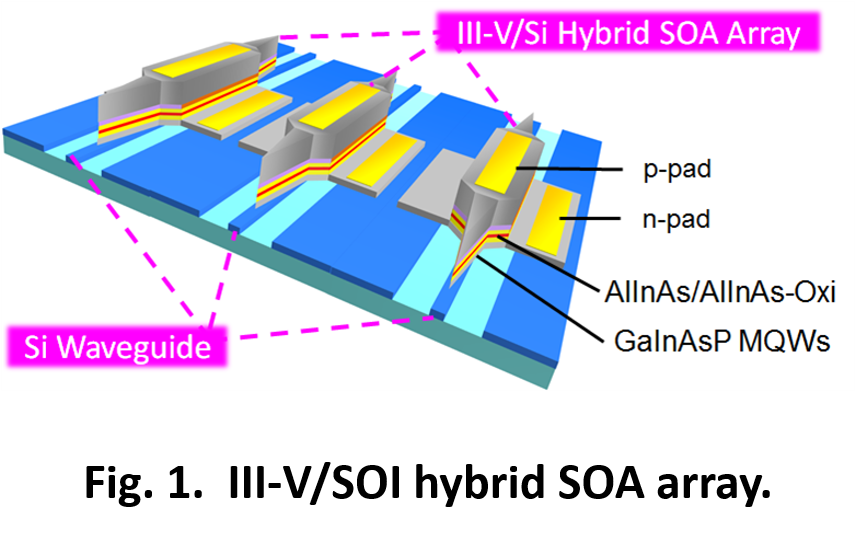 |
近年のインターネットトラヒックの増大に伴い、高効率・大容量な光ルーティング機能を有する大規模な光集積回路が求められています。そのアプローチとして、Siプラットフォーム上へIII-V族半導体による光源や増幅器といった光アクティブデバイスを作製するIII-V/Siハイブリッド集積が有効です。Siは通信波長帯において透明で低損失かつ小型の光回路を作製できることに加えて、CMOSプロセスを利用した低コストで大規模な光電集積が可能であり、InPなどのIII-V族半導体は直接遷移半導体であるため、間接遷移半導体のSiでは作製困難な発光デバイスを実現できます。本グループでは、ハイブリッド集積におけるInP光源とSi光回路それぞれの特性とそれらを組み合わせた構造に着目し、InPもしくはSiだけでは実現困難な多機能な光集積回路をの実現を目指しています。
|
| |
| |
| II. III-V/SOI窒素プラズマ活性化接合 |
| |
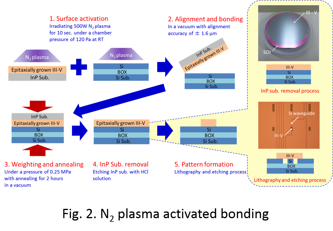
SiとIII-V族半導体という異種材料の接合には、低温で高強度な接合が可能な窒素プラズマ活性化接合という手法を用います。両基板の表面に付着した酸化膜や吸着層をプラズマ照射によって除去し、加熱加重を行うことで接合を行います(Fig. 2)。接合温度150°Cにおいて90%以上の貼り付け面積を達成しています。さらに、Si構造や表面処理を工夫することで、Si導波路を形成した場合の貼り付けであっても同等の貼り付け面積に加えて貼り付け界面のボイドを大幅に削減できています。本プロセスを基にしてハイブリッド集積の実現を目指します。
|
| |
 |
| |
| III. III-V/Siハイブリッドレーザ |
| |
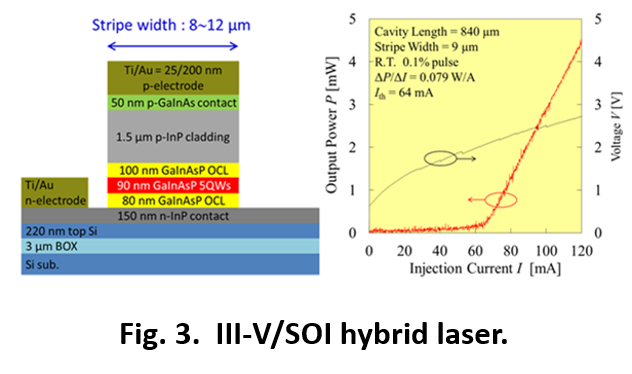
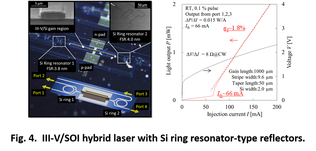
| 窒素プラズマ活性化接合を用いたハイブリッドレーザの電流注入動作を達成し、しきい値電流密度0.85 kA/cm2と従来のハイブリッドレーザと比較して良好な発振特性を得ています(Fig. 3)。またSi光回路との集積に向けて、Si導波路によるリング共振器型ミラーを導入したハイブリッドレーザの作製を行っています(Fig. 4)。2つのリング共振器型ミラーの温度変調による広い波長可変領域、長い外部共振器構造による狭い発振線幅の実現を目指します。さらにAlInAs層酸化による高効率動作実現にも取り組んでいます。
|
 |
 |
|
| |
| IV. III-V/Siハイブリッド集積 |
| |
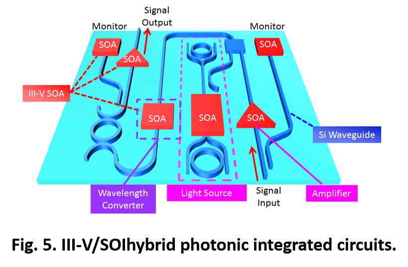
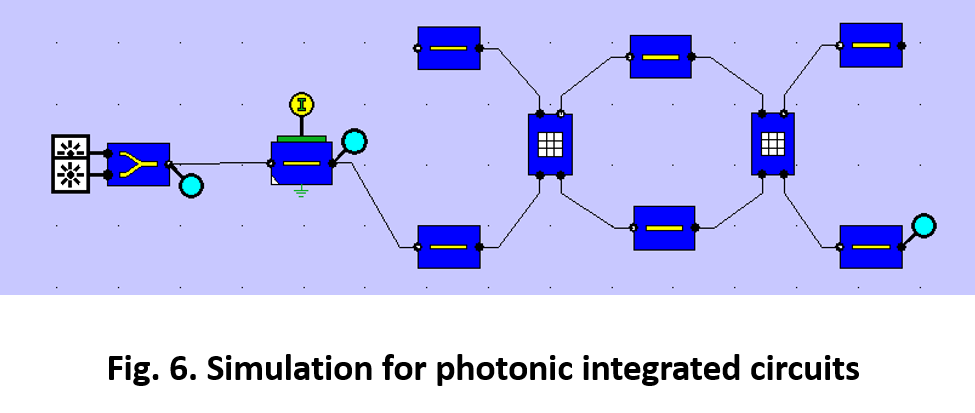
| ハイブリッド集積のために、Si光導波路上にGaInAsP/InP光源を作製する必要があり、上記の直接貼り付け技術に加えて、本研究室のもつ導波路作製技術を組み合わせて光ルーティング機能やWDM送受信機といった多機能な大規模光集積回路を実現します(Fig. 5)。また大規模光集積回路の設計に要する複雑な計算の簡易化に向けた、設計シミューレーション法の構築も行っています(Fig. 6)。
|
 |
 |
|
|
| |
| List of reports |
| Journal Papers |
(1) T. Maruyama, T. Okumura, S. Sakamoto, K. Miura, Y. Nishimoto, and S. Arai: “GaInAsP/InP membrane BH-DFB lasers directly bonded on SOI substrate,” Opt. Express, Vol. 16, No. 14, pp. 8814-8818, Sep. 2006.
(2) T. Maruyama, T. Okumura, and S. Arai: “Direct wafer bonding of GaInAsP/InP membrane structure on silicon-on-insulator substrate,” Jpn. J. Appl. Phys., Vol. 45, No. 11, pp. L8717-L8718, Nov. 2006.
(3) T. Okumura, T. Maruyama, M. Kanemaru, S. Sakamoto, and S. Arai:“Single-modeoperation of GaInAsP/InP-membrane distributed feedback (DFB) lasers bonded on silicon-on-insulator (SOI) substrate with rib-waveguide structure,” Jpn. J. Appl. Phys., Vol. 46, No. 48, pp. L1206-L1208, Dec. 2007.
(4) T. Okumura, T. Maruyama, H. Yonezawa, N. Nishiyama, and S. Arai: “Injection-type GaInAsP/InP/Si Distributed-feedback Laser Directly Bonded on Silicon-on-insulator Substrate,” IEEE Photon. Technol. Lett. Vol. 21, No. 5, pp. 283-285, Mar. 2009.
(5) R. Osabe, T. Okumura, S. Kondo, N. Nishiyama, and S. Arai.“Bonding and Photoluminescence Characteristics of GaInAsP/InP Membrane Structure on Silicon-on-Insulator Waveguides by Surface Activated Bonding,” Jpn. J. Appl . Phys., vol. 50, No. 8, pp. 088005-1-2, Aug. 2011.
(6) Y. Hayashi, R. Osabe, K. Fukuda, Y. Atsumi, N. Nishiyama, and S. Arai. “Low Threshold Current Density Operation of a GaInAsP/Si Hybrid Laser Prepared by Low-Temperature N2 Plasma Activated Bonding,” Jpn. J. Appl. Phys., Vol. 52, pp. 060202-1-3, June 2013.
(7) J. Suzuki, Y. Hayashi, Y. Kuno, J. Kang, T. Amemiya, N. Nishiyama, and S. Arai. “Surface assessment after removing III-V layer on III-V/silicon-on-insulator wafer fabricated by plasma activated bonding,” Jpn. J. Appl. Phys., Vol. 53, pp. 118003-1-3, Oct. 2014.
|
| |
International Conferences |
(1) T. Maruyama, T. Okumura, S. Sakamoto, K. Miura, Y. Nishimoto, and S. Arai: “Direct bonding of GaInAsP/InP membrane structure on SOI wafer,” The 18th Indium Phosphide and Related Materials Conference (IPRM2006), Princeton (USA), WP-2, May 2006.
(2) T. Okumura, T. Maruyama, M. Kanemaru, S. Sakamoto, S. Tamura, and S. Arai: “Fundamental-mode operation of GaInAsP/InP membrane DFB lasers bonded on SOI substrate and its waveguide integration,” The 19th Indium Phosphide and Related Material (IPRM 2007), Matsue (Japan), TuB2-2, May 2007.
(3) T. Maruyama, T. Okumura, M. Kanemaru, S. Sakamoto, S. Tamura, and S. Arai: “Thermal characteristics of GaInAsP/InP membrane DFB lasers on SOI substrate integrated with rib-waveguide,” The 12th Opto-Electronics and Communications Conference (OECC 2007), Yokohama (Japan), 12D1-3, July 2007.
(4) T. Maruyama, T. Okumura, S. Sakamoto, K. Miura, Y. Nishimoto, and S. Arai: “GaInAsP/InP long-wavelength membrane BH-DFB lasers directly bonded on SOI Substrate,” The 11th Opto-Electronics and Communications Conference (OECC 2007), Yokohama (Japan), 12D1-3, July 2007.
(5) T. Okumura, T. Maruyama, H. Yonezawa, N. Nishiyama, and S. Arai: “Injection Type GaInAsP/InP/Si DFB Lasers Directly Bonded on SOI Substrate,” The 20th Indium Phosphide and Related Material (IPRM 2008), Versailles (France), TuA1-6, May 2008.
(6) S. Kondo, T. Okumura, R. Osabe, N. Nishiyama, and S. Arai, “Investigation of Bonding Strength and Photoluminescence Properties of InP/Si Surface Activated Bonding.” The 22th International Conference on Indium Phosphide and Related Materials (IPRM2010), Kagawa (Japan), WeP28, May. 2010.
(7) R. Osabe, T. Okumura, S. Kondo, N. Nishiyama, and S. Arai, “Stabilization on Fabrication of GaInAsP/InP Membrane Structure on SOI waveguide by Surface Activated Bonding.” The 37th International Symposium on Compound Semiconductors (ISCS 2010), Kagawa (Japan), FrP23, May. 2010.
(8) Y. Hayashi, R. Osabe, K. Fukuda, N. Nishiyama, and S. Arai, “GaInAsP/Si Hybrid Fabry-Perot Laser using N2 Plasma Activated Low Temperature Bonding.” 2012 IEEE Photonics Conference (IPC2012), California (USA), ThO4, Sep. 2012.
(9) Y. Hayashi, R. Osabe, K. Fukuda, N. Nishiyama, S. Arai, “Design of Multi-Functional GaInAsP/Si Hybrid Semiconductor Optical Amplifier Array with AlInAs-Oxide Current Confinement Layer,” The 25th Int. Conf. on Indium Phosphide and Related Materials (IPRM-2013), Kobe, Japan, TuD3-4, May 2013.
(10) Y. Hayashi, J. Suzuki, Y. Kuno, J. Kang, T. Amemiya, N. Nishiyama, and S. Arai, “Investigation of High Temperature Process for III-V/SOI Hybrid Photonic Devices with AlInAs Oxidation Current Confinement Layer,” 4th IEEE International Workshop on Low Temperature Bonding for 3D Integration (LTB-3D 2014), Tokyo, Japan, July 2014.
(11) J. Suzuki, Y. Hayashi, Y. Kuno, J. Kang, T. Amemiya, N. Nishiyama, and S. Arai, “Light Propagation Properties of Si Waveguides after Removing III-V Layer on a III-V/SOI Wafer Fabricated by Plasma Activated Bonding,” 4th IEEE International Workshop on Low Temperature Bonding for 3D Integration (LTB-3D 2014), Tokyo, Japan, July 2014.
|
| |
| Meeting Reports and Symposia |
(1) S. Arai, T. Maruyama, N. Nishiyama, T. Okumura, M. Kurokawa, M. Shirao, Y. Yonezawa, D. Kondo, H. Ito “Membrane Semiconductor Lasers on SOI Substrates”, 「SOI上の半導体薄膜レーザ」 Technical Meeting of IEICE, SiPH2008-15, pp.19-24, Tokyo (Japan), Nov. 2008.
(2) T. Okumura, T. Maruyama, H. Yonezawa, N. Nishiyama, and S. Arai, “Electrically pumped GaInAsP/InP DFB Laser on SOI Substrate by Direct Wafer Bonding” Technical Report of IEICE, LQE2008-29, pp. 45-50, Tokyo (Japan), Jun. 2008.
(3) T. Maruyama, T. Okumura, H. Yonezawa, N. Nishiyama, and S. Arai:“GaInAsP/InP membrane DFB laser on SOI substrate using direct wafer bonding, “International Symposium on VCSELs and Integrated Photonic,” P-13, pp.138-139, Tokyo (Japan), Dec. 2007.
(4) T. Okumura, T. Maruyama, H. Yonezawa, N. Nishiyama, and S. Arai:“Single-mode and high temperature operation of GaInAsP/InP membrane DFB lasers on SOI substrate and its waveguide integration, “International Symposium on VCSELs and Integrated Photonic,” P-14, pp. 140-141, Tokyo (Japan), Dec. 2007.
(5) T. Maruyama, T. Okumura, M. Kanemaru, S. Sakamoto, and S. Arai: “GaInAsP/InP membrane BH-DFB lasers integrated with waveguide structure on SOI substrate” Technical Meeting of IEICE, SiPH2006-11, pp.49-52, Tokyo (Japan), Jan. 2007.
(6) T. Okumura, T. Maruyama, S. Sakamoto, Y. Nishimoto, and S. Arai: “GaInAsP/InP membrane BH-DFB lasers on SOI substrate by direct bonding” Technical Report of IEICE, LQE2006-104, pp. 7-10, Tokyo (Japan), Dec. 2006
(7) 林 侑介、鈴木純一、渥美裕樹、姜 晙炫、西山伸彦、荒井滋久:「AlInAs酸化電流狭窄型GaInAsP/SOIハイブリッドレーザ構造の直接貼り付け・高温プロセスの検討」、電子情報通信学会 シリコンフォトニクス研究会(SiPH)、東京、P18、2013年10月18日
(8) J. Suzuki, Y. Hayashi, J. Kang, Y. Atsumi, N. Nishiyama and S. Arai, “Design of Si Ring-Resonator-Type Reflector for GaInAsP/SOI Hybrid Laser,” The 3rd International Symposium on Photonics and Electronics Convergence, ISPEC2013, Tokyo, Japan, P-8, Nov. 2013.
(9) 鈴木純一、林 侑介、渥美裕樹、姜 晙炫、西山伸彦、荒井滋久:「InP/Siハイブリッド光デバイスにおける複数光機能一括貼り付け形成のための構造検討」、電子情報通信学会 レーザ・量子エレクトロニクス研究会(LQE)、東京、Technical Report of IEICE、LQE2013-129、Vol. 113、No. 352、pp. 21-26、2013年12月13日
(10) Y. Hayashi, J. Suzuki, S. Inoue, J. Kang, Y. Kuno, T. Amemiya, N. Nishiyama and S. Arai, “GaInAsP/SOI Hybrid Laser with Ring-resonator-type Reflector Fabricated by Plasma Activated Bonding,” The 4th International Symposium on Photonics and Electronics Convergence, ISPEC2014, Tokyo, Japan, P-8, Nov. 2014
(11) 林 侑介、鈴木純一、久能 雄輝、姜 晙炫、雨宮 智宏、西山伸彦、荒井滋久:「N2プラズマ活性化貼付法で作製したリング共振器ミラー装荷型GaInAsP/SOIハイブリッドレーザ」、電子情報通信学会 光通信システム研究会(OCS)、東京、Technical Report of IEICE、OCS2014-129、Vol. 113、No. 352、pp. 21-26、2014年12月12日
|
| |
Domestic Conferences |
(1) T. Maruyama, T. Okumura, and S. Arai: “Direct bonding of GaInAsP/InP membrane structure on SOI substrate,” The 53rd Spring Meeting, 2006; The Japan Society of Applied Physics and Related Societies, 24a-B-6, p. 1472, Tokyo, Mar. 2006
(2) T. Maruyama, T. Okumura, S. Sakamoto, and S. Arai: “GaInAsP/InP membrane DFB laser on SOI substrate by direct wafer bonding method,” The 67th Autumn Meeting, 2006; The Japan Society of Applied Physics, 29a-ZT-15, p. 1049, Shiga, Aug. 2006.
(3) T. Maruyama, T. Okumura, M. Kanemaru, S. Sakamoto, and S. Arai: “GaInAsP/InP membrane DFB lasers on SOI substrate integrated with waveguide structure,” The 54th Spring Meeting, 2007; The Japan Society of Applied Physics and Related Societies, 28a-SG-11, p. 1221, Kanagawa, Mar. 2007.
(4) T. Okumura, T. Maruyama, M. Kanemaru, and S. Arai: “GaInAsP/InP light emitting diode on SOI substrate by direct wafer bonding,” The 68th Autumn Meeting, 2007; The Japan Society of Applied Physics, 7a-C-13, p. 1160, Sapporo, Sep. 2007.
Nobuhiko Nishiyama, Takeo Maruyama and Shigehisa Arai:「シリコン基板上半導体レーザ・発光デバイスの現状」(依頼講演)、The 2009 IEICE General Conference, CI-2-4, Ehime, Mar. 2009.
(5) T. Maruyama, T. Okumura, and S. Arai: “A perspective for the realization of semiconductor laser on silicon substrate (invited),” the 2007 IEICE Society Conference, CK-1-8, Tottori, Sep. 2007.
Shigehisa Arai:「Active Photonic Devices on SOI Substrates」(Tutorial)、The 2008 IEICE Society Conference, CT-1-2, Kanagawa, Sept. 2008.
(6) T. Okumura, T. Maruyama, H. Yonezawa, N. Nishiyama, and S. Arai: ”Injection Type GaInAsP/InP DFB Laser on SOI Substrate by Direct Wafer Bonding”, The 55th Spring Meeting, 2008; The Japan Society of Applied Physics and Related Societies, 29p-ZQ-4, Digest III-p. 1208, Chiba, Mar. 2008.
(7) S. Arai:「Active Photonic Devices on SOI Substrates」(Tutorial)、The 2008 IEICE Society Conference, CT-1-2, Kanagawa, Sep. 2008.
(8) Nobuhiko Nishiyama, Takeo Maruyama and Shigehisa Arai:「シリコン基板上半導体レーザ・発光デバイスの現状」(依頼講演)、The 2009 IEICE General Conference, CI-2-4, Ehime, Mar. 2009.
(9) S. Kondo, T. Okumura, R. Osabe, N. Nishiyama, and S. Arai, 「表面活性化貼付法を用いたInP/Si 接合とフォトルミネッセンス特性」 The 57th Spring Meeting 2010; The Japan Society of Applied Physics and Related Societies, 17p-P3-13, Kanagawa, Mar. 2010.
(10) N. Nishiyama, S. Arai, T. Okumura, H. Ito, H. Enomoto, S. Kondo, Y. Maeda, R. Osabe, and T. Amemiya 「Si/III-Vハイブリッド光デバイスと関連技術」 日本学術振興会半導体界面制御技術第154委員会研究会, May. 2010.
(11) R.Osabe, T. Okumura, S. Kondo, N. Nishiyama, and S. Arai, 「表面活性化接合法によるSOI導波路上GaInAsP薄膜構造の形成」 The 71st Autumn Meeting, The Japan Society of Applied Physics and Related Societies, 14p-G-15, Nagasaki, Sep. 2010.
(12) N. Nishiyama, T. Okumura, and S. Arai, 「Si・SOI基板上レーザ素子の現状」 レーザー学会学術講演会第31回年次大会, Tokyo, 10p-v-05, Jan. 2011.
(13) K. Fukuda, R.Osabe, Y. Atsumi, N. Nishiyama, and S. Arai, 「Si導波路幅の制御によるGaInAsP/SiハイブリッドSOA 多機能集積のための設計」 The 72nd Autumn Meeting, The Japan Society of Applied Physics and Related Societies, 31p-ZN-5, Yamagata, Aug. 2011.
(14) R.Osabe, K. Fukuda, M. Shirao, N. Nishiyama, and S. Arai, 「AlInAs酸化狭窄層を有するGaInAsP/InP-Siハイブリッドレーザの構造設計」The 72nd Autumn Meeting, The Japan Society of Applied Physics and Related Societies, 1p-ZL-1, Yamagata, Aug. 2011.
(15) K. Fukuda, R.Osabe, Y. Atsumi, N. Nishiyama, and S. Arai, 「AlInAs酸化狭窄層を有するGaInAsP/SiハイブリッドSOA多機能集積のための構造設計」 The 2012 Society Conference, C-3-62, Toyama, Sep. 2012.
(16) Y. Hayashi, R. Osabe, K. Fukuda, Y. Atsumi, J. H. Kang, N. Nishiyama, and S. Arai, 「表面活性化接合を用いたGaInAsP/Siハイブリッドファブリペローレーザ」 The 73rd Autumn Meeting, The Japan Society of Applied Physics and Related Societies, 12a-C6-8, Ehime, Sep. 2012.
(17) 鈴木純一、林 侑介、渥美裕樹、姜 晙炫、西山伸彦、荒井滋久:「AlInAs酸化電流狭窄型GaInAsP/SOI ハイブリッドレーザ構造の高温プロセスによる影響」、第74回春季応用物理学会学術講演会、京田辺、19a-P2-1、2013年09月16日~2013年09月20日
(18) 鈴木純一、林 侑介、久能 雄輝、姜 晙炫、雨宮 智宏、西山伸彦、荒井滋久:「表面活性化接合を用いたIII?V/SOIハイブリッド光デバイスにおけるIII?V層部分エッチングプロセスの検討」、第75回秋季応用物理学会学術講演会、札幌、18a-A18-3、2014年09月17日~2013年09月20日
(19) 林 侑介、鈴木純一、久能 雄輝、姜 晙炫、雨宮 智宏、西山伸彦、荒井滋久:「プラズマ活性化貼付法を用いたリング共振器ミラー装荷型GaInAsP/SOIハイブリッドレーザの作製」、電気情報通信学会 2014年ソサイエティ大会、徳島、C-4-15、2014年09月23日~2013年09月26日
| | △ このページのトップ △ |
| |
| |
|
| |
|