 |
| Research |
| I. III-V/SOI optical integrated circuit |
 |
In recent years, with the rapid increasing of internet traffic, researches are being done to produce large-scale Optical Integrated Circuit possessing high efficient and high capacity optical routing tool. AS an approach, to manufacture optically active devices like optical source and amplifier using III-V semiconductors on Si platform ‘III-V/Si Hybrid Integration process’ is available. Si is a transparent and low-loss medium within communication wavelength band and small-size optical circuit can be manufactured using Si, it is possible to do large-scale integration by CMOS process at low cost. As III-V group semiconductors like InP are direct-bandgap semiconductors, it is possible to realize optical devices using III-V semiconductors which will be difficult to realize using indirect-bandgap Si. In this group, we emphasize on the characteristics of each InP optical source and Si optical waveguides and use their combined structure to realize multi-function optical integrated circuit which is difficult to realize with only InP or Si.
|
| |
| II. III-V/SOI N2 plasma activated bonding |
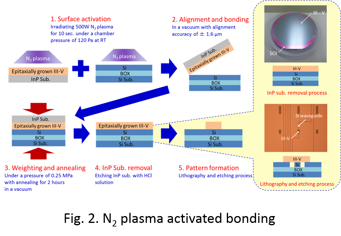
For the bonding of different materials like Si and III-V group semiconductor, in low temperature high strength bonding is achievable using N2 plasma activated bonding method. After removing oxide film and adsorption layer by plasma irradiation from both of the substrates’ surfaces, bonding is done by heated-weighting (Fig. 2). At 150° bonding temperature over 90% bonding-area is achieved. Moreover by devising Si structure and surface treatment process, during the bonding of waveguide formed Si substrate void between bonded interfaces is largely reduced. |
| |
 |
| |
| III. III-V/Si hybrid laser |
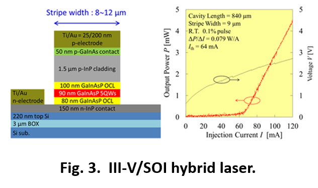
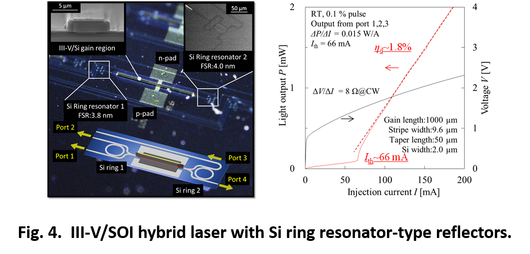
| We confirmed the current injection operation of hybrid laser manufactured by N2 plasma activated bonding method. Threshold current density of 0.85kA/cm2 and favorable lasing characteristic comparing with traditional hybrid lasers is achieved (Fig. 3). With the goal of integration with Si optical circuit, we are manufacturing hybrid laser by introducing Si waveguide formed ring-resonator type reflector on both sides (Fig 4). The target is to achieve wide wavelength variable region due to the two ring-resonator type reflectors’ temperature modulation and realization of narrow lasing spectrum due to external long cavity. We are also working on realizing high-efficiency operation by narrowing AlInAs layer using oxidation method. |
 |
 |
|
|
| IV. III-V/Si hybrid optical integration |
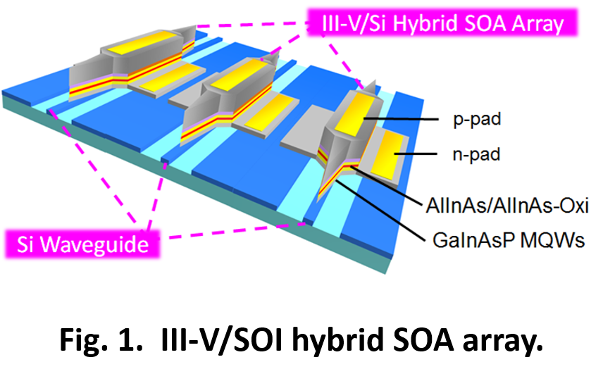
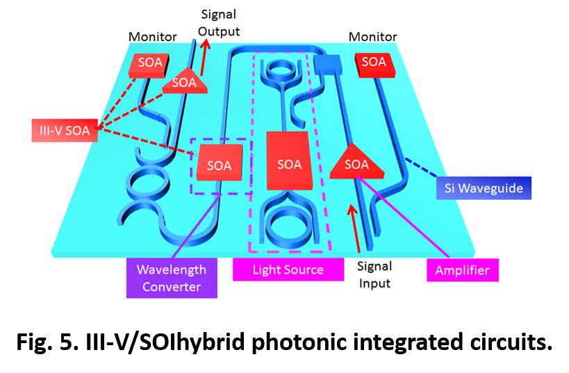
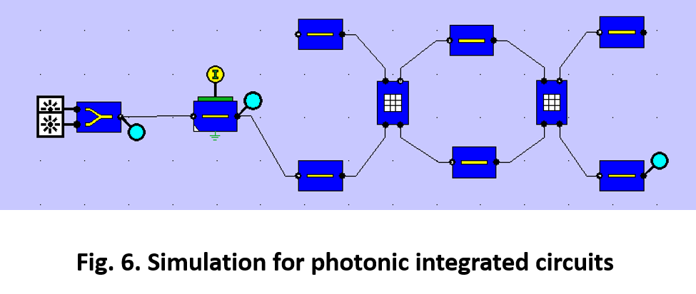
| For hybrid integration, it is necessary to fabricate GaInAsP/InP optical source over Si waveguide. We will realize multipurpose large-scale optical integrated circuit like optical routing tool and WDM transceiver by previously described direct bonding method combining with waveguide fabrication method cultivated in our lab (Fig. 5). We are also constructing the designing and simulation process of optical integrated circuit with the goal of simplifying complicated calculation needed for designing large-scale optical integrated circuit (Fig 6).
|
 |
 |
| |
| List of reports |
| Journal Papers |
(1) T. Maruyama, T. Okumura, S. Sakamoto, K. Miura, Y. Nishimoto, and S. Arai: “GaInAsP/InP membrane BH-DFB lasers directly bonded on SOI substrate,” Opt. Express, Vol. 16, No. 14, pp. 8814-8818, Sep. 2006.
(2) T. Maruyama, T. Okumura, and S. Arai: “Direct wafer bonding of GaInAsP/InP membrane structure on silicon-on-insulator substrate,” Jpn. J. Appl. Phys., Vol. 45, No. 11, pp. L8717-L8718, Nov. 2006.
(3) T. Okumura, T. Maruyama, M. Kanemaru, S. Sakamoto, and S. Arai:“Single-modeoperation of GaInAsP/InP-membrane distributed feedback (DFB) lasers bonded on silicon-on-insulator (SOI) substrate with rib-waveguide structure,” Jpn. J. Appl. Phys., Vol. 46, No. 48, pp. L1206-L1208, Dec. 2007.
(4) T. Okumura, T. Maruyama, H. Yonezawa, N. Nishiyama, and S. Arai: “Injection-type GaInAsP/InP/Si Distributed-feedback Laser Directly Bonded on Silicon-on-insulator Substrate,” IEEE Photon. Technol. Lett. Vol. 21, No. 5, pp. 283-285, Mar. 2009.
(5) R. Osabe, T. Okumura, S. Kondo, N. Nishiyama, and S. Arai.“Bonding and Photoluminescence Characteristics of GaInAsP/InP Membrane Structure on Silicon-on-Insulator Waveguides by Surface Activated Bonding,” Jpn. J. Appl . Phys., vol. 50, No. 8, pp. 088005-1-2, Aug. 2011.
(6) Y. Hayashi, R. Osabe, K. Fukuda, Y. Atsumi, N. Nishiyama, and S. Arai. “Low Threshold Current Density Operation of a GaInAsP/Si Hybrid Laser Prepared by Low-Temperature N2 Plasma Activated Bonding,” Jpn. J. Appl. Phys., Vol. 52, pp. 060202-1-3, June 2013.
(7) J. Suzuki, Y. Hayashi, Y. Kuno, J. Kang, T. Amemiya, N. Nishiyama, and S. Arai. “Surface assessment after removing III-V layer on III-V/silicon-on-insulator wafer fabricated by plasma activated bonding,” Jpn. J. Appl. Phys., Vol. 53, pp. 118003-1-3, Oct. 2014.
|
| |
International Conferences |
(1) T. Maruyama, T. Okumura, S. Sakamoto, K. Miura, Y. Nishimoto, and S. Arai: “Direct bonding of GaInAsP/InP membrane structure on SOI wafer,” The 18th Indium Phosphide and Related Materials Conference (IPRM2006), Princeton (USA), WP-2, May 2006.
(2) T. Okumura, T. Maruyama, M. Kanemaru, S. Sakamoto, S. Tamura, and S. Arai: “Fundamental-mode operation of GaInAsP/InP membrane DFB lasers bonded on SOI substrate and its waveguide integration,” The 19th Indium Phosphide and Related Material (IPRM 2007), Matsue (Japan), TuB2-2, May 2007.
(3) T. Maruyama, T. Okumura, M. Kanemaru, S. Sakamoto, S. Tamura, and S. Arai: “Thermal characteristics of GaInAsP/InP membrane DFB lasers on SOI substrate integrated with rib-waveguide,” The 12th Opto-Electronics and Communications Conference (OECC 2007), Yokohama (Japan), 12D1-3, July 2007.
(4) T. Maruyama, T. Okumura, S. Sakamoto, K. Miura, Y. Nishimoto, and S. Arai: “GaInAsP/InP long-wavelength membrane BH-DFB lasers directly bonded on SOI Substrate,” The 11th Opto-Electronics and Communications Conference (OECC 2007), Yokohama (Japan), 12D1-3, July 2007.
(5) T. Okumura, T. Maruyama, H. Yonezawa, N. Nishiyama, and S. Arai: “Injection Type GaInAsP/InP/Si DFB Lasers Directly Bonded on SOI Substrate,” The 20th Indium Phosphide and Related Material (IPRM 2008), Versailles (France), TuA1-6, May 2008.
(6) S. Kondo, T. Okumura, R. Osabe, N. Nishiyama, and S. Arai, “Investigation of Bonding Strength and Photoluminescence Properties of InP/Si Surface Activated Bonding.” The 22th International Conference on Indium Phosphide and Related Materials (IPRM2010), Kagawa (Japan), WeP28, May. 2010.
(7) R. Osabe, T. Okumura, S. Kondo, N. Nishiyama, and S. Arai, “Stabilization on Fabrication of GaInAsP/InP Membrane Structure on SOI waveguide by Surface Activated Bonding.” The 37th International Symposium on Compound Semiconductors (ISCS 2010), Kagawa (Japan), FrP23, May. 2010.
(8) Y. Hayashi, R. Osabe, K. Fukuda, N. Nishiyama, and S. Arai, “GaInAsP/Si Hybrid Fabry-Perot Laser using N2 Plasma Activated Low Temperature Bonding.” 2012 IEEE Photonics Conference (IPC2012), California (USA), ThO4, Sep. 2012.
(9) Y. Hayashi, R. Osabe, K. Fukuda, N. Nishiyama, S. Arai, “Design of Multi-Functional GaInAsP/Si Hybrid Semiconductor Optical Amplifier Array with AlInAs-Oxide Current Confinement Layer,” The 25th Int. Conf. on Indium Phosphide and Related Materials (IPRM-2013), Kobe, Japan, TuD3-4, May 2013.
(10) Y. Hayashi, J. Suzuki, Y. Kuno, J. Kang, T. Amemiya, N. Nishiyama, and S. Arai, “Investigation of High Temperature Process for III-V/SOI Hybrid Photonic Devices with AlInAs Oxidation Current Confinement Layer,” 4th IEEE International Workshop on Low Temperature Bonding for 3D Integration (LTB-3D 2014), Tokyo, Japan, July 2014.
(11) J. Suzuki, Y. Hayashi, Y. Kuno, J. Kang, T. Amemiya, N. Nishiyama, and S. Arai, “Light Propagation Properties of Si Waveguides after Removing III-V Layer on a III-V/SOI Wafer Fabricated by Plasma Activated Bonding,” 4th IEEE International Workshop on Low Temperature Bonding for 3D Integration (LTB-3D 2014), Tokyo, Japan, July 2014.
|
| |
| Meeting Reports and Symposia |
(1) S. Arai, T. Maruyama, N. Nishiyama, T. Okumura, M. Kurokawa, M. Shirao, Y. Yonezawa, D. Kondo, H. Ito “Membrane Semiconductor Lasers on SOI Substrates”, 「SOI上の半導体薄膜レーザ」 Technical Meeting of IEICE, SiPH2008-15, pp.19-24, Tokyo (Japan), Nov. 2008.
(2) T. Okumura, T. Maruyama, H. Yonezawa, N. Nishiyama, and S. Arai, “Electrically pumped GaInAsP/InP DFB Laser on SOI Substrate by Direct Wafer Bonding” Technical Report of IEICE, LQE2008-29, pp. 45-50, Tokyo (Japan), Jun. 2008.
(3) T. Maruyama, T. Okumura, H. Yonezawa, N. Nishiyama, and S. Arai:“GaInAsP/InP membrane DFB laser on SOI substrate using direct wafer bonding, “International Symposium on VCSELs and Integrated Photonic,” P-13, pp.138-139, Tokyo (Japan), Dec. 2007.
(4) T. Okumura, T. Maruyama, H. Yonezawa, N. Nishiyama, and S. Arai:“Single-mode and high temperature operation of GaInAsP/InP membrane DFB lasers on SOI substrate and its waveguide integration, “International Symposium on VCSELs and Integrated Photonic,” P-14, pp. 140-141, Tokyo (Japan), Dec. 2007.
(5) T. Maruyama, T. Okumura, M. Kanemaru, S. Sakamoto, and S. Arai: “GaInAsP/InP membrane BH-DFB lasers integrated with waveguide structure on SOI substrate” Technical Meeting of IEICE, SiPH2006-11, pp.49-52, Tokyo (Japan), Jan. 2007.
(6) T. Okumura, T. Maruyama, S. Sakamoto, Y. Nishimoto, and S. Arai: “GaInAsP/InP membrane BH-DFB lasers on SOI substrate by direct bonding” Technical Report of IEICE, LQE2006-104, pp. 7-10, Tokyo (Japan), Dec. 2006
(7) 林 侑介、鈴木純一、渥美裕樹、姜 晙炫、西山伸彦、荒井滋久:「AlInAs酸化電流狭窄型GaInAsP/SOIハイブリッドレーザ構造の直接貼り付け・高温プロセスの検討」、電子情報通信学会 シリコンフォトニクス研究会(SiPH)、東京、P18、2013年10月18日
(8) J. Suzuki, Y. Hayashi, J. Kang, Y. Atsumi, N. Nishiyama and S. Arai, “Design of Si Ring-Resonator-Type Reflector for GaInAsP/SOI Hybrid Laser,” The 3rd International Symposium on Photonics and Electronics Convergence, ISPEC2013, Tokyo, Japan, P-8, Nov. 2013.
(9) 鈴木純一、林 侑介、渥美裕樹、姜 晙炫、西山伸彦、荒井滋久:「InP/Siハイブリッド光デバイスにおける複数光機能一括貼り付け形成のための構造検討」、電子情報通信学会 レーザ・量子エレクトロニクス研究会(LQE)、東京、Technical Report of IEICE、LQE2013-129、Vol. 113、No. 352、pp. 21-26、2013年12月13日
(10) Y. Hayashi, J. Suzuki, S. Inoue, J. Kang, Y. Kuno, T. Amemiya, N. Nishiyama and S. Arai, “GaInAsP/SOI Hybrid Laser with Ring-resonator-type Reflector Fabricated by Plasma Activated Bonding,” The 4th International Symposium on Photonics and Electronics Convergence, ISPEC2014, Tokyo, Japan, P-8, Nov. 2014
(11) 林 侑介、鈴木純一、久能 雄輝、姜 晙炫、雨宮 智宏、西山伸彦、荒井滋久:「N2プラズマ活性化貼付法で作製したリング共振器ミラー装荷型GaInAsP/SOIハイブリッドレーザ」、電子情報通信学会 光通信システム研究会(OCS)、東京、Technical Report of IEICE、OCS2014-129、Vol. 113、No. 352、pp. 21-26、2014年12月12日
|
| |
Domestic Conferences |
(1) T. Maruyama, T. Okumura, and S. Arai: “Direct bonding of GaInAsP/InP membrane structure on SOI substrate,” The 53rd Spring Meeting, 2006; The Japan Society of Applied Physics and Related Societies, 24a-B-6, p. 1472, Tokyo, Mar. 2006
(2) T. Maruyama, T. Okumura, S. Sakamoto, and S. Arai: “GaInAsP/InP membrane DFB laser on SOI substrate by direct wafer bonding method,” The 67th Autumn Meeting, 2006; The Japan Society of Applied Physics, 29a-ZT-15, p. 1049, Shiga, Aug. 2006.
(3) T. Maruyama, T. Okumura, M. Kanemaru, S. Sakamoto, and S. Arai: “GaInAsP/InP membrane DFB lasers on SOI substrate integrated with waveguide structure,” The 54th Spring Meeting, 2007; The Japan Society of Applied Physics and Related Societies, 28a-SG-11, p. 1221, Kanagawa, Mar. 2007.
(4) T. Okumura, T. Maruyama, M. Kanemaru, and S. Arai: “GaInAsP/InP light emitting diode on SOI substrate by direct wafer bonding,” The 68th Autumn Meeting, 2007; The Japan Society of Applied Physics, 7a-C-13, p. 1160, Sapporo, Sep. 2007.
Nobuhiko Nishiyama, Takeo Maruyama and Shigehisa Arai:「シリコン基板上半導体レーザ・発光デバイスの現状」(依頼講演)、The 2009 IEICE General Conference, CI-2-4, Ehime, Mar. 2009.
(5) T. Maruyama, T. Okumura, and S. Arai: “A perspective for the realization of semiconductor laser on silicon substrate (invited),” the 2007 IEICE Society Conference, CK-1-8, Tottori, Sep. 2007.
Shigehisa Arai:「Active Photonic Devices on SOI Substrates」(Tutorial)、The 2008 IEICE Society Conference, CT-1-2, Kanagawa, Sept. 2008.
(6) T. Okumura, T. Maruyama, H. Yonezawa, N. Nishiyama, and S. Arai: ”Injection Type GaInAsP/InP DFB Laser on SOI Substrate by Direct Wafer Bonding”, The 55th Spring Meeting, 2008; The Japan Society of Applied Physics and Related Societies, 29p-ZQ-4, Digest III-p. 1208, Chiba, Mar. 2008.
(7) S. Arai:「Active Photonic Devices on SOI Substrates」(Tutorial)、The 2008 IEICE Society Conference, CT-1-2, Kanagawa, Sep. 2008.
(8) Nobuhiko Nishiyama, Takeo Maruyama and Shigehisa Arai:「シリコン基板上半導体レーザ・発光デバイスの現状」(依頼講演)、The 2009 IEICE General Conference, CI-2-4, Ehime, Mar. 2009.
(9) S. Kondo, T. Okumura, R. Osabe, N. Nishiyama, and S. Arai, 「表面活性化貼付法を用いたInP/Si 接合とフォトルミネッセンス特性」 The 57th Spring Meeting 2010; The Japan Society of Applied Physics and Related Societies, 17p-P3-13, Kanagawa, Mar. 2010.
(10) N. Nishiyama, S. Arai, T. Okumura, H. Ito, H. Enomoto, S. Kondo, Y. Maeda, R. Osabe, and T. Amemiya 「Si/III-Vハイブリッド光デバイスと関連技術」 日本学術振興会半導体界面制御技術第154委員会研究会, May. 2010.
(11) R.Osabe, T. Okumura, S. Kondo, N. Nishiyama, and S. Arai, 「表面活性化接合法によるSOI導波路上GaInAsP薄膜構造の形成」 The 71st Autumn Meeting, The Japan Society of Applied Physics and Related Societies, 14p-G-15, Nagasaki, Sep. 2010.
(12) N. Nishiyama, T. Okumura, and S. Arai, 「Si・SOI基板上レーザ素子の現状」 レーザー学会学術講演会第31回年次大会, Tokyo, 10p-v-05, Jan. 2011.
(13) K. Fukuda, R.Osabe, Y. Atsumi, N. Nishiyama, and S. Arai, 「Si導波路幅の制御によるGaInAsP/SiハイブリッドSOA 多機能集積のための設計」 The 72nd Autumn Meeting, The Japan Society of Applied Physics and Related Societies, 31p-ZN-5, Yamagata, Aug. 2011.
(14) R.Osabe, K. Fukuda, M. Shirao, N. Nishiyama, and S. Arai, 「AlInAs酸化狭窄層を有するGaInAsP/InP-Siハイブリッドレーザの構造設計」The 72nd Autumn Meeting, The Japan Society of Applied Physics and Related Societies, 1p-ZL-1, Yamagata, Aug. 2011.
(15) K. Fukuda, R.Osabe, Y. Atsumi, N. Nishiyama, and S. Arai, 「AlInAs酸化狭窄層を有するGaInAsP/SiハイブリッドSOA多機能集積のための構造設計」 The 2012 Society Conference, C-3-62, Toyama, Sep. 2012.
(16) Y. Hayashi, R. Osabe, K. Fukuda, Y. Atsumi, J. H. Kang, N. Nishiyama, and S. Arai, 「表面活性化接合を用いたGaInAsP/Siハイブリッドファブリペローレーザ」 The 73rd Autumn Meeting, The Japan Society of Applied Physics and Related Societies, 12a-C6-8, Ehime, Sep. 2012.
(17) 鈴木純一、林 侑介、渥美裕樹、姜 晙炫、西山伸彦、荒井滋久:「AlInAs酸化電流狭窄型GaInAsP/SOI ハイブリッドレーザ構造の高温プロセスによる影響」、第74回春季応用物理学会学術講演会、京田辺、19a-P2-1、2013年09月16日~2013年09月20日
(18) 鈴木純一、林 侑介、久能 雄輝、姜 晙炫、雨宮 智宏、西山伸彦、荒井滋久:「表面活性化接合を用いたIII?V/SOIハイブリッド光デバイスにおけるIII?V層部分エッチングプロセスの検討」、第75回秋季応用物理学会学術講演会、札幌、18a-A18-3、2014年09月17日~2013年09月20日
(19) 林 侑介、鈴木純一、久能 雄輝、姜 晙炫、雨宮 智宏、西山伸彦、荒井滋久:「プラズマ活性化貼付法を用いたリング共振器ミラー装荷型GaInAsP/SOIハイブリッドレーザの作製」、電気情報通信学会 2014年ソサイエティ大会、徳島、C-4-15、2014年09月23日~2013年09月26日
| | △ このページのトップ △ |
| |
| |
|
| |
|
| |
 |