| Research |
|
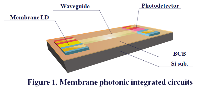
■Membrane photonic integrated circuits
-Membrane DFB laser
-Membrane waveguide
|
| |
| Research |
| Membrand DFB laser |
|
| A membrane structure with high index contrast (HIC) which enables ultra-small and highly integrated optical circuits is very attractive to the ultralow power consumption light sources. The refractive index difference between semiconductor core and low index polymer cladding layer is about 40%, which enhanced the optical field in its core layer compared with that of conventional double hetero structures. A semiconductor membrane laser which composed of thin (150 nm) core and polymer claddings, shows 3 times higher optical confinement factor due to the HIC effect.
|
| |
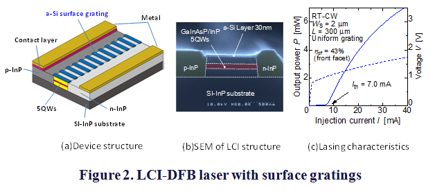
| 1) Lateral current injection (LCI) structure
|
| |
|
| |
| A very low threshold operation was realized in the optically pumped membrane laser, but an external light source is required in this system, which is not preferable for the device integration. It is difficult to combine the membrane and vertical pn-junction structure as mentioned before. Then, we introduced a lateral current injection (LCI) structure which has lateral pn-junction to our membrane based devices. Up to now, we have realized LCI laser on semi-insulated substrate with GaInAsP thin (400 nm) core layers including 5 quantum wells by organic metallic vapor phase epitaxy regrowth technique. Moreover as shown in Fig 2, the DFB laser with LCI structure was fabricated and characterized with low threshold operation. In this structure, because the bottom cladding layer was semi-insulated InP substrate, the optical confinement factor was weaker than the membrane structure. Then, investigations for electrical and optical properties are currently in progress in the membrane DFB laser with LCI structure.
|
| |
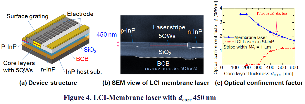
| 2) Membrane DFB laser with LCI structure
|
| |
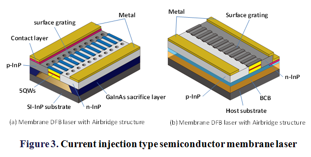 |
| For membrane laser with LCI structure, it is important to form Ⅲ-Ⅴ compound semiconductor thin film (membrane) on low refractive index cladding layer such as SiO2 or air. Towards the realization of LCI-membrane laser with ultra low threshold operation, the two types of laser have been proposed and researched; the air-bridge structure and Ⅲ-Ⅴsemiconductor bonded to SiO2 structure using BCB adhesive wafer bonding.
|
 |
| |
| △ Top to the page △ |
| |
| |
| |
| List of reports |
| Journal Papers |
(1) T. Okamoto, N. Nunoya, Y. Onodera, S. Tamura and S.
Arai, “Continuous wave operation of optically pumped membrane
DFB laser,” Ellectron. Lett., vol. 37, no. 24, pp. 1455-1456,
Nov. 2001.
(2) T. Okamoto, N. Nunoya, Y. Onodera, S. Tamura and S. Arai,
“Single-Mode Operation of Optically Pumped Membrane Buried
Heterostructure Distributed-Feedback Lasers,” Jpn. J. Appl.
Phys., vol. 41, no. 3A, pp. L249-L251, Mar. 2002.
(3) T. Okamoto, N. Nunoya, Y. Onodera, S. Tamura and S. Arai,
“Low-Threshold Singlemode Operation of Membrane BH-DFB Lasers,”
Ellectron. Lett., vol. 38, no. 23, pp. 1444-1446, Nov. 2002.
(4) T. Okamoto, N. Nunoya, Y. Onodera, T. Yamazaki, S. Tamura
and S. Arai, “Optically Pumped Membrane BH-DFB Lasers for
Low-Threshold and Single-Mode Operation,” IEEE J. Select.
Topics in Quantum Electron., vol. 9, no. 5, pp. 1361-1366,
Sept. /Oct. 2003.
(5) T. Okamoto, T. Yamazaki, S. Sakamoto, S. Tamura and S.
Arai, “Low Threshold Membrane BH-DFB Laser Arrays with Precisely
Controlled Wavelength over a Wide Range,” IEEE Photon. Technol.
Lett., vol. 15, no. 5, pp. 1242-1244, May 2004.
(6) S. Sakamoto, T. Okamoto, T. Yamazaki, S. Tamura and S.
Arai, “Multiple-Wavelengths Membrane BH-DFB Laser Arrays,”
IEEE J. Select. Topics in Quantum Electronics, No. 11, Vol.
5, pp. 1174-1179, Sep. /Oct. 2005.
(7) S. Sakamoto, H. Naitoh, M. Ohtake, Y. Nishimoto, T. Maruyama, N. Nishiyama, and S. Arai, “85°C Continuous-Wave Operation of GaInAsP/InP-Membrane Buried Heterostructure Distributed Feedback Lasers with Polymer Cladding Layer,” Jpn. J. Appl. Phys., vol. 46, no. 47, pp. 1155-1157, Nov. 2007
(8) H. Naitoh, S. Sakamoto, Mamoru Otake, T. Okumura, T. Maruyama, N. Nishiyama, and S. Arai, “GaInAsP/InP Membrane Buried Heterostructure Distributed Feedback Laser with Air-Bridge Structure,” Jpn. J. Appl. Phys., vol. 46, no. 47, pp. 1158-1160, Nov. 2007.
5, pp. 1174-1179, Sep. /Oct. 2005.
(9) S. Sakamoto, Y. Nishimoto, S. Tamura, T. Maruyama, N. Nishiyama, and S. Arai, “Strongly Index-Coupled Membrane BH-DFB Lasers With Surface Corrugation Grating,” IEEE J. Select. Top. in Quantum Electron., vol. 13, no. 5, pp. 1135-1141, Sep. 2007.
(10) T. Okumura, M. Kurokawa, M. Shirao, D. Kondo, H. Ito, N. Nishiyama, T. Maruyama, and S. Arai, “Lateral current injection GaInAsP/InP laser on semi-insulating substrate for membrane-based photonic circuits,” Opt. Express, Vol. 17, No. 15, pp. 12564-12570, Jul. 2009.
(11) T. Okumura, H. Ito, D. Kondo, N. Nishiyama, and S. Arai, “Continuous Wave Operation of Thin Film Lateral Current Injection Lasers Grown on Semi-insulating InP,” Jpn. J. Appl. Phys., vol. 49, no. 4, pp. 040205, Apr. 2010.
(12) S. Arai, N. Nishiyama, T. Maruyama, and T. Okumura, “GaInAsP/InP Membrane Lasers for Optical Interconnects,” IEEE J. Sel. Top. Quantum Electron., vol. 17, no. 5, pp. 1381-1389, Sep. 2011.
(13) T. Shindou, T. Okumura, H. Ito, T. Koguchi, D. Takahashi, Y. Atsumi, J. Kang, R. Osabe, T. Amemiya, N. Nishiyama, and S. Arai, “Lateral-Current-Injection Distributed Feedback Laser with Surface Grating Structure,” IEEE J. Sel. Top. Quantum Electron., vol. 17, no. 5, pp. 1175-1182, Sep. 2011.
(14) T. Okumura, D. Kondo, H. Ito, S. Lee, T. Amemiya, N. Nishiyama, and S. Arai, “Lateral Junction Waveguide-Type Photodiode Grown on Semi-Insulating InP Substrate,” Jpn. J. Appl. Phys., vol. 50, no. 2, pp. 020206-1-020206-3, Feb. 2011.
(15) T. Shindou, T. Okumura, H. Ito, T. Koguchi, D. Takahashi, Y. Atsumi, J. Kang, R. Osabe, T. Amemiya, N. Nishiyama, and S. Arai, “GaInAsP/InP lateral-current-injection distributed feedback laser with a-Si surface grating,” Opt. Express, vol. 19, no. 3, pp. 1884-1891, Jan. 2011
(16) M. Futami, T. Shindo, T. Koguchi, K. Shinno, T. Amemiya, N. Nishiyama, and S. Arai, “GaInAsP/InP Lateral Current Injection Laser with Uniformly Distributed Quantum Well Structure,” IEEE Photonics Technol. Lett., vol. 24, no. 11, pp. 888-890, Jun. 2012.
|
| |
| International Conferences |
| (1) T. Okamoto, N. Nunoya, Y. Onodera, S. Tamura and S.
Arai, “CW Operation of Optically Pumped Membrane DFB Laser,”
The 4th Pacific Rim Conf. On Lasers and Electro-Optics (CLEO/PR2001),
WJPD1-10, pp.44-45 (PD), Makuhari Chiba, Japan), July 2001.
(2) T. Okamoto, N. Nunoya, Y. Onodera, S. Tamura and S. Arai,
“Single Mode Operation of Optically Pumped Membrane BH-DFB
Lasers,” The 14th Annual Meeting of The IEEE Lasers &
Electro-Optics Society (LEOS2001), PD1.1, San Diego (USA),
Nov. 2001.
(3) T. Okamoto, N. Nunoya, Y. Onodera, S. Tamura and S. Arai,
“1550nm Wavelength Membrane DFB Laser Cladded by BCB Polymer,”
5th International Symposium on Contemporary Photonics Technology
(CPT2002), Tokyo, E-21, pp. 101-102, Jan. 2002.
(4) T. Okamoto, N. Nunoya, Y. Onodera, S. Tamura and S. Arai,
“Low threshold operation of membrane buried heterostructure
distributed feedback laser,” 14th Indium Phosphide and Related
Materials Conf. (IPRM2002), Stockholm, PI-4, pp.115-118, May,
2002.
(5) T. Okamoto, Y. Onodera, T. Yamazaki, S. Tamura and S.
Arai, “Membrane Distributed Feedback Lasers for Ultra Low
Threshold Current Operation,” The 9th Int'l Symposium on Quantum
Effect Electronics, 9, pp. 58-61, Tokyo, Nov. 2002.
(6) T. Okamoto, Y. Onodera, T. Yamazaki, S. Tamura and S.
Arai, “Low Threshold Membrane BH-DFB Laser Arrays for 1490-1565nm
Wavelength Range,” 15th Indium Phosphide and Related Materials
Conf. (IPRM2003), Santa Barbara, FA2.5, pp. 558-561, May,
2003.
(7) S. Arai, T. Okamoto, Y. Onodera, T. Yamazaki, S. Tamura,
“Low Threshold GaInAsP/InP Membrane BH-DFB Lasers,” (Invited),
The 8th Optoelectronics and Communications Conference (OECC2003),
Shanghai, Oct. 2003.
(8) T. Okamoto, T. Yamazaki, S. Sakamoto, S. Tamura and S.
Arai, “Low Threshold Operation of Optically Pumped Membrane
BH-DFB Laser Arrays with a Wide Wavelength Range,” The 16th
Annual Meeting of The IEEE Lasers & Electro-Optics Society
(LEOS2003), WT 2, pp. 636-637, Tucson (USA), Oct. 2003.
(9) T. Okamoto, T. Yamazaki, S. Sakamoto, S. Tamura and S.
Arai, “Short Cavity Membrane BH-DFB Laser with l/4
Phase Shift,” 16th Indium Phosphide and Related Materials
Conf. (IPRM2004), WA-3-3, pp. 519-523, Kagoshima, May, 2004.
(10) T. Okamoto, T. Yamazaki, S. Sakamoto, S. Tamura and S.
Arai, “Improved Temperature Insensitivity of Membrane BH-DFB
Laser with Polymer Cladding Layers”, The 9th Optoelectronics
and Communication Conference (OECC2004), 14E2-3, pp. 528-529,
Yokohama, July, 2004.
(11) T. Okamoto, T. Yamazaki, S. Sakamoto, S. Tamura and S.
Arai, “Multiple-Wavelengths Low-Threshold Membrane BH-DFB
Laser Arrays”, 2004 IEEE 19th International Semiconductor
Laser Conference, WC1, Matsue, Sept., 2004.
(12) S. Sakamoto, T. Okamoto, T. Yamazaki, H. Kawashima, Tang
Jing-Long, S. Tamura and S. Arai, “Narrow Stripe Membrane
BH-DFB Lasers for Lateral-Mode Control,” The 6th Pacific Rim
Conf. On Lasers and Electro-Optics (CLEO/PR2005), CTuJ 4-6,
Tokyo, July 2005
(13) S. Sakamoto, H. Kawashima, H. Naitoh, S. Tamura, T. Maruyama
and S. Arai, “Narrow Stripe Membrane BH-DFB Lasers with Surface
Corrugation for Stable Single-Mode Operation”, The 18th International
Conference on Indium Phosphide and Related Materials (IPRM2006),
TuA1-7, Princeton, USA, May 2006.
(14) S. Sakamoto, H. Kawashima, H. Naitoh, S. Tamura, T. Maruyama
and S. Arai, “Narrow Stripe Membrane BH-DFB Lasers with Surface
Corrugation for Stable Single-Mode Operation”, The 11th International
Conference on Optical Electrical Comunication Conference (OECC2006),5E1-3,
Kaohsiung, Taiwan, July 2006.
(15) S. Sakamoto, H. Naitoh, H. Kawashima, Y. Nishimoto, S.
Tamura, T. Maruyama and S. Arai, “1-step OMVPE Grown Strongly
Index-Coupled Membrane DFB Laser with Surface Corrugation
Grating Structure,” 2006 IEEE 19th International Semiconductor
Laser Conference (ISLC2006),P 10, Hawai, USA, Sep. 2006.
(16) H. Naitoh, S. Sakamoto, M. Otake, T. Okumura, T. Maruyama, N. Nishiyama, and S. Arai, “80 oC CW Operation of GaInAsP/InP Membrane BH-DFB Laser With Air-Bridge Structure,” The 19th Indium Phosphide and Related Material (IPRM 2007), Matsue (Japan), ThB1-2, May. 2007.
(17) S. Sakamoto, H. Naitoh, H. Kawashima, M. Ohtake, S. Tamura, T. Maruyama, N. Nishiyama, and S. Arai, “85℃ continuous wave operation of membrane BH-DFB Laser cladded by benzocyclobutene,” 10th International Symposium on Contemporary Photonics Technology (CPT 2007), Tokyo (Japan), G-6, Jan. 2007.
(18) T. Okumura, M. Kurokawa, M. Shirao, D. Kondo, N. Nishiyama, and S. Arai, “Top-Air-Cladding GaInAsP/InP Lateral Current Injection Type Lasers,” IEEE Nanotechnology Materials and Device Conference 2008, MoC I-5, Oct. 2008.
(19) T. Okumura, M. Kurokawa, M. Shirao, D. Kondo, H. Ito, N. Nishiyama, and S. Arai, “GaInAsP/InP Lateral Current Injection Laser Grown on SI-InP Substrate,” 2008 International Nano-Optoelectronics Workshop, session3-P27, Aug. 2008.
(20) H. Ito, T. Okumura, D. Kondo, N. Nishiyama, and S. Arai, “Improved Quantum Efficiency of Lateral Current Injection Type Fabry-Perot Lasers,” International Symposium on Quantum Nanophotonics and Nanoelectronics, University of Tokyo, ThC-4, Nov. 2009.
(21) T. Okumura, M. Kurokawa, D. kondo, H. Ito, N. Nishiyama, and S. Arai, “Lateral Current Injection Type GaInAsP/InP DFB Lasers on SI-InP Substrate,” The 21st International Conference on Indium Phosphide and Related Materials (IPRM2009), Newport Beach, California, TuB2, May. 2009.
(22) T. Okumura, M. Kurokawa, H. Ito, D. kondo, N. Nishiyama, and S. Arai, “Room-Temperature CW Operation of Lateral Current Injection Lasers with Thin Film Lateral,” The 21st International Conference on Indium Phosphide and Related Materials (IPRM2009), Newport Beach, California, WP 12, May. 2009.
(23) T. Shindou, T. Okumura, H. Ito, T. Koguchi, D. Takahashi, Y. Atsumi, J. Kang, R. Osabe, N. Nishiyama, and S. Arai, “Lateral Current Injection Type GaInAsP/InP DFB Laser with a-Si Surface Grating,” The 23rd Annual Meeting of the IEEE Photonics Society, Denver, USA, ThR 4, Nov. 2010.
(24) . Okumura, T. Koguchi, H. Ito, N. Nishiyama, S. Arai, “First Lasing Operation of Injection Type Membrane GaInAsP DFB Laser With Lateral Current Injection BH Structure,” the 22nd IEEE International Semiconductor Laser Conference, Kyoto, Japan, ThB-2, Sep. 2010
(25) H. Ito, T. Okumura, D. kondo, N. Nishiyama, and S. Arai, “Thin-Film GaInAsP/InP Lateral Current Injection Type Fabry-Perot Laser Improved Quantum Efficiency Operation,” The 22th International Conference on Indium Phosphide and Related Materials (IPRM2010), Takamatsu, Japan, TuA3-5, Jun. 2010.
(26) D. Kondo, T. Okumura, H. Ito, S. Lee, T. Amemiya, N. Nishiyama, and S. Arai, “Lateral Junction Waveguide Type Photodiode for Membrane Photonic Circuits,” International Conference on Indium Phosphide and Related Materials, The 22nd International Conference on Indium Phosphide and Related Materials (IPRM2010), May. 2010.
(27) T. Okumura, D. Kondo, H. Ito, S. Lee, D. Takahashi, N. Nishiyama, and S. Arai, “Dynamic Characteristics of Lateral Current Injection Laser,” The 37th International Symposium on Compound Semiconductors (ISCS 2010), Kagawa, Japan, WeE3-2, May. 2010.
(29) S. Arai, N. Nishiyama, T. Okumura, “Membrane DFB Laser on SOI,” Asia Communications and Photonics Conference and Exhibition 2010 (ACP2010), Shanghai, China, ThF1, Dec. 2010.
(30) S. Arai, and N. Nishiyama, “Membrane-Type Photonic Devices for Optical Circuits on SOI,” 2010 Sokid State Devices and Materials, D-6-1, Sep. 2010.
(31) N. Nishiyama, and S. Arai, “Membrane InP-based Lasers and Related Devices for On-chip Interconnects,” IEEE Photonics Photonics 2011, WA3, Nov. 2011.
(32) T. Shindo, M. Futami, R. Osabe, T. Koguchi, T. Amemiya, N. Nishiyama, and S. Arai, “Lateral Current Injection Laser with Uniformly Distributed Quantum-Well Structure,” 2011 IEEE Photonics Conference (IPC-2011), ThC3, Oct. 2011.
(33) M. Futami, T. Shindo, T. Okumura, R. Osabe, D. Takahashi, T. Koguchi, T. Amemiya, N. Nishiyama, and S. Arai, “Stripe Width Dependence of Internal Quantum Efficiency and Carrier Injection Delay in Lateral Current Injection GaInAsP/InP Lasers,” The 16th Opto-Electronics and Communication Conference (OECC-2011), 7D2-2, Jul. 2011.
(34) T. Shindo, M. Futami, T. Okumura, R. Osabe, T. Koguchi, T. Amemiya, N. Nishiyama, and S. Arai, “Lasing Operation of Lateral-Current-Injection Membrane DFB Laser with Surface Grating,” The 16th Opto-Electronics and Communication Conference, 6D3-7, Jul. 2011.
(35) T. Shindo, T. Okumura, M. Futami, R. Osabe, T. Koguchi, T. Amemiya, N. Nishiyama, and S. Arai, “Lateral Current Injection Distributed Feedback Laser with Wirelike Active Regions,” The 23rd International Conference on Indium Phosphide and Related Materials (IPRM-2011), Tu5.2-3, May. 2011
(36) S. Arai, N. Nishiyama, T. Okumura, and T. Shindou. “Lateral current injection GaInAsP/InP laser for membrane based photonic circuits,” SPIE Photonics West Conference 2011, San Francisco, California, (USA), 7953-06, Jan. 2011.
(37) T. Shindo, M. Futami, K. Doi, T. Amemiya, N. Nishiyama, and S. Arai, “Modulation Bandwidth of GaInAsP/InP Lateral-Current-Injection Membrane Laser,” 23rd IEEE International Semiconductor Laser Conference (ISLC 2012), TuP17, Oct. 2012.
(38) K. Doi, T. Shindou, M. Futami, T. Amemiya, N. Nishiyama, and S. Arai, “Thermal Analysis of Self-Heating Effect in GaInAsP/InP Membrane DFB Laser on Si Substrate,” 2012 IEEE Photonics Conference (IPC-2012), ThO2, Sep. 2012.
(39) M. Futami, T. Shindo, K. Doi, T. Amemiya, N. Nishiyama, and S. Arai, “Low-Threshold Operation of LCI-Membrane-DFB Lasers with Be-doped GaInAs Contact Layer,” 24th International Conference on Indium Phosphide and Related Materials (IPRM 2012), Th-2C.5, Aug. 2012.
(40) T. Shindo, T. Koguchi, M. Futami, K. Shinno, K. Doi, T. Amemiya, N. Nishiyama, and S. Arai, “10 Gb/s Operation of GaInAs/InP Top Air-Clad. Lateral Junction Waveguide-type Photodiode,” 2012 IEEE Optical Interconnects Conference (OIC-2012), TuP2, May. 2012.
(41) M. Futami, K. Shinno, T. Shindo, K. Doi, T. Amemiya, N. Nishiyama, and S. Arai, “Improved Quantum Efficiency of GaInAsP/InP Top Air-Clad Lateral Current Injection Lasers,” 2012 IEEE Optical Interconnects Conference (OIC-2012), TuB3, May. 2012
|
| |
| Meeting Report |
| (1) T. Okamoto, Y. Onodera, T. Yamazaki, S. Tamura and
S. Arai, “A Study of Semiconductor Membrane BH-DFB Laser Arrays,”
「半導体薄膜BH-DFBレーザに関する研究」 Technical Report of IEICE, OPE2003-30
(2003-07), pp.35-38, Tokyo (Japan), July 2003.
(2) T. Okamoto, T. Yamazaki, S. Sakamoto, S. Tamura and S.
Arai, “Polymer Cladded Semiconductor Membrane BH-DFB Lasers,”
「誘電体クラッド半導体薄膜BH-DFBレーザ」 Technical Report of IEICE, OPE2004-20
(2004-07), pp.11-14, Tokyo (Japan), July 2004.
(3) S. Sakamoto, H. Naitoh, S. Tamura, T. Maruyama and S.
Arai, “Membrane BH-DFB Laser with Surface Corrugation Grating”,
「凹凸形状回折格子を用いた半導体薄膜BH-DFBレーザ」, Technical Report of IEICE, OPE2006-19
(2004-06), pp.1-6, Tokyo (Japan), June 2006.
|
| |
| Domestic Conferences |
| (1) K. Matsui, T. Okamoto, N. Nunoya and S. Arai, “Analysis
of threshold current of membrane DFB lasers with wirelike
active regions,” 「半導体薄膜活性層分離型DFBレーザの閾値電流解析」 Nat. Conv. Res.
of Japan Soc. Appl. Phys., 30a-ZS-7, Digest III pp. 1152,
Tokyo, Mar. 2001.
(2) T. Okamoto, N. Nunoya, Y. Onodera, S. Tamura and S. Arai,
“Room Temperature CW Operation of Optically-Pumped Membrane
DFB Lasers,” 「半導体薄膜構造DFBレーザの光励 起室温連続動作」 Nat. Conv. Res. of
Japan Soc. Appl. Phys., 13p-B-14, Digest III pp. 869, Aichi,
Sep. 2001.
(3) T. Okamoto, N. Nunoya, Y. Onodera, S. Tamura and S. Arai,
“Single-Mode Operation of Optically Pumped Membrane BH-DFB
Lasers,” 「BH構造を導入した光励起半導体薄膜DFBレーザの単一モード動作」 Nat. Conv. Res.
of Japan Soc. Appl. Phys., 29a-YS-9, Digest III pp. 1144,
Kanagawa, Mar. 2002.
(4) Y. Onodera, T. Okamoto, N. Nunoya, S. Tamura and S. Arai,
“Low Threshold Operation of Membrane BH-DFB Lasers,” 「半導体薄膜DFBレーザの低しきい値動作」
Nat. Conv. Res. of Japan Soc. Appl. Phys., 29a-YS-9, Digest
III pp. 1144, Kanagawa, Mar. 2002.
(5) T. Okamoto, Y. Onodera, T. Yamazaki, S. Tamura and S.
Arai, “Proposal of Multiple Wavelength Membrane DFB Laser
Array,” 「位相シフト変調型半導体薄膜DFB多波長アレイ光源の提案」Nat. Conv. Res. of Japan
Soc. Appl. Phys., 26p-A-12, Digest III pp. 996, Niigata, Sep.
2002.
(6) T. Okamoto, Y. Onodera, T. Yamazaki, S. Tamura and S.
Arai, “Wavelength Controllability of Membrane BH-DFB Lasers,”
「半導体薄膜BH-DFBレーザの波長制御性」 Nat. Conv. Res. of Japan Soc. Appl.
Phys., 28p-ZQ-16, Digest III pp. 1241, Kanagawa, Mar. 2003.
(7) T. Okamoto, Y. Onodera, T. Yamazaki, S. Tamura and S.
Arai, “Fabrication of Multiple Wavelength Membrane BH-DFB
Laser Arrays,” 「半導体薄膜BH-DFB多波長レーザアレイの試作」Nat. Conv. Res. of
Japan Soc. Appl. Phys., 28p-ZQ-17, Digest III pp. 1241, Kanagawa,
Mar. 2003.
(8) T. Okamoto, T. Yamazaki, S. Tamura and S. Arai, “Room
Temperature CW Operation of Phase Shifted Membrane BH-DFB
Laser,” 「位相シフト半導体薄膜BH-DFBレーザの室温連続動作」Nat. Conv. Res. of Japan
Soc. Appl. Phys., 30p-YB-11, Digest III pp. 1041, Fukuoka,
Aug. 2003.
(9) T. Yamazaki, T. Okamoto, S. Tamura and S. Arai, “Low Threshold
Operation of Membrane BH-DFB Laser Arrays,” 「半導体薄膜BH-DFBレーザアレイの低しきい値動作」
Nat. Conv. Res. of Japan Soc. Appl. Phys., 30p-YB-12, Digest
III pp. 1042, Fukuoka, Aug. 2003.
(10) T. Okamoto, T. Yamazaki, S. Sakamoto, S. Tamura and S.
Arai, “Athermal effect of polymer cladded membrane BH-DFB
laser,” 「誘電体クラッドを用いた半導体薄膜BH-DFBレーザにおけるアサーマル効果の観測」Nat. Conv.
Res. of Japan Soc. Appl. Phys., 30a-ZZ-5, Digest III pp. 1260,
Tokyo, Mar. 2004.
(11) T. Yamazaki, T. Okamoto, S. Sakamoto, S. Tamura and S.
Arai, “Multiple wavelength membrane BH-DFB laser arrays,”
「一括励起半導体薄膜BH-DFB多波長レーザアレイの試作」Nat. Conv. Res. of Japan Soc.
Appl. Phys., 30a-ZZ-6, Digest III pp. 1260, Tokyo, Mar. 2004.
(12) S. Sakamoto, T. Okamoto, T. Yamazaki, S. Tamura and S.
Arai, “Athermal effect of polymer cladded membrane BH-DFB
laser,” 「誘電体クラッドを用いた半導体薄膜BH-DFBレーザにおけるアサーマル効果の観測」Nat. Conv.
Res. of Japan Soc. Appl. Phys., 1a-ZN-9, Digest III Miyagi,
Sept. 2004.
(13) T. Okamoto, S. Sakamoto, T. Yamazaki, S. Tamura and S.
Arai, “Membrane BH-DFB laser array with exposure control,”
「EB露光量制御による微小波長間隔半導体薄膜BH-DFBレーザアレイ」Nat. Conv. Res. of Japan
Soc. Appl. Phys., 1a-ZN-10, Digest III Miyagi, Sept. 2004.
(14) T. Okamoto, S. Sakamoto, T. Yamazaki, S. Tamura and S.
Arai, “Membrane BH-DFB Laser with High Index Difference Waveguide”,
「高屈折率差導波路構造を用いた半導体薄膜BH-DFBレーザ」, The 65th Autumn Meeting, 2004;
The Japan Society of Applied Physics., 1a-ZN-10, Digest III
-p. 1020, Sendai, Sep. 2004.
(15) S. Sakamoto, T. Okamoto, T. Yamazaki, H. Kawashima, Tang
Jing-Long, S. Tamura and S. Arai, “Membrane BH-DFB Laser Array
with Asperity Corrugation Structure”, 「凹凸形状回折格子を用いた半導体薄膜BH-DFBレーザアレイ」,
The 52nd Spring Meeting, 2005; The Japan Society of Applied
Physics and Related Societies., 31p-ZH-5, Saitama, Mar./Apr.
2005.
(16) H. Kawashima, S. Sakamoto, T. Okamoto, T. Yamazaki, Tang
Jing-Long, S. Tamura and S. Arai, “Lateral-Mode Control of
Membrane BH-DFB Lasers with Narrow Stripe”, 「狭ストライプ半導体薄膜BH-DFBレーザの横モード制御」,
The 52nd Spring Meeting, 2005; The Japan Society of Applied
Physics and Related Societies.,31p-ZH-6, Saitama, Mar./Apr.
2005.
(17)S. Sakamoto, H. Kawashima, H. Naitoh, S. Tamura, T. Maruyama,
and S. Arai, “Narrow Stripe Membrane BH-DFB Laser Array using
Surface Corrugation”「凹凸形状回折格子を用いた狭ストライプ半導体薄膜BH-DFBレーザアレイ」,
The 53rd Spring Meeting, 2006; The Japan Society of Applied
Physics and Related Societies.,23a-Za-4, Tokyo, Mar. 2006.
(18)S. Sakamoto, H. Naitoh, H. Kawashima, Y. Nishimoto, S.
Tamura, T. Maruyama, and S. Arai, “High Temperature Continuous
Wave Operation of Membrane BH-DFB Laser”「 半導体薄膜BH-DFBレーザの高温連続動作」,
The 67th Autumn Meeting, 2006; The Japan Society of Applied
Physics., 29a-ZT-5, Digest III pp.1046 , Shiga, Aug. 2006.
(19)S. Sakamoto, H. Naitoh, H. Kawashima, S. Tamura, T. Maruyama,
and S. Arai, “Low Threshold Operation of Short Cavity Membrane
BH-DFB Laser using Surface Corrugation Grating”「凹凸形状回折格子を用いた短共振器半導体薄膜BH-DFBレーザの低しきい値動作」,
The 67th Autumn Meeting, 2006; The Japan Society of Applied
Physics., 29a-ZT-6, Digest III pp.1046 , Shiga, Aug. 2006.
(20)H. Naitoh, S. Sakamoto, H. Kawashima, Y. Nishimoto, S.
Tamura, T. Maruyama, and S. Arai, “1-step OMVPE Grown Index
Coupled Membrane DFB Laser with Surface Corrugation Structure,”「1回OMVPE成長による凹凸形状半導体薄膜DFBレーザ」,
The 67th Autumn Meeting, 2006; The Japan Society of Applied
Physics., 29a-ZT-7, Digest III pp.1047 , Shiga, Aug. 2006.
|
| |
| Awards |
(1) T. Okamoto, “Continuous Wave Operation of Optically Pumped
Membrane DFB Laser,” Student Paper Contest, Third Place, IEEE
Student Branch at Tokyo Institute of Technology, Dec. 2001.
(2) T. Okamoto, “Membrane Distributed Feedback Lasers for Ultra
Low Threshold Current Operation,” Student Paper Contest, Third
Place, IEEE Student Branch at Tokyo Institute of Technology,
Dec. 2002.
(3) T. Okamoto, “Low Threshold and Precisely Wavelength Controlled
Membrane BH-DFB Laser Arrays with a Wide Wavelength Range,”
Student Paper Contest, First Place, IEEE Student Branch at Tokyo
Institute of Technology, Dec. 2003.
(4) 岡本健志 「位相シフト半導体薄膜BH-DFBレーザの室温連続動作」 第15回応用物理学会講演奨励賞2004年3月.
(5) 黒川宗高 「OMVPE再成長法による薄膜クラッド層を有する横方向電流注入型レーザ」 第25回応用物理学会講演奨励賞2008年9月
|
| |
| △ このページのトップ △ |
| |
| |
| |
| Research |
| Membrane waveguide |
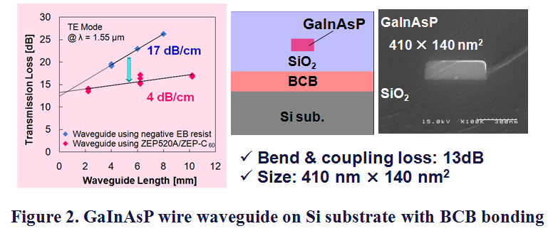
| To realize the membrane photonic integrated circuits (PICs) on Si-LSI, it is necessary to transmit optical signal from light sources with low propagation loss. For the waveguide, we have investigate the membrane wire waveguide which has thin InP-based core buried SiO2 by BCB adhesive wafer bonding, with back-end CMOS process. Because of its membrane wire structure, it has the low bend loss and small foot-print.
|
| |
| 1) BCB adhesive wafer bonding process
|
| |

|
| |
| For the BCB bonding process, as illustrated in Fig. 1, organo-metallic vapor-phase epitaxy was used to grow an InP wafer that consisted of a 150-nm-thick of Ga0.21In0.79As0.46P0.54 (λg = 1.22 μm) core layer on top of double etch-stop layers (InP/GaInAs). Then, a SiO2 bottom cladding layer was deposited on the InP substrate by plasma-enhanced chemical-vapor deposition (PECVD). Meanwhile, a Si wafer was spin-coated with BCB, which was then thermally pre-cured to remove solvent and induce polymerization for adhesion. Both wafers were then bonded under vacuum, in the next step, the BCB layer was completely solidified by hard-curing. Finally, the InP substrate and stack of etch-stop layers (InP/GaInAs) were removed by selective wet etching to leave behind the exposed GaInAsP membrane on the Si substrate.
|
| |
| 2) GaInAsP wire waveguide on Si substrate
|
| |
|
| |
| With BCB bonding and EB lithography, the GaInAsP wire waveguide on Si substrate was fabricated and the propagation loss was as low as 4 dB/cm. In order to realize the membrane PICs, the reduction of propagation loss, the application to optical functional devices and the integration with laser have been researched.
|
| |
| List of reports |
| Journal Papers |
(1) J. Lee, Y. Maeda, Y. Atsumi, Y. Takino, N. Nishiyama, and S. Arai, “Low-loss GaInAsP wire waveguide on Si substrate with Benzocyclobutene adhesive wafer bonding for membrane photonic circuits,” Jpn. J. App. Phys., Vol. 51, pp. 042201-1 ? 042201-5, Apr. 2012.
|
| |
| International Conferences |
| (1) Y. Maeda, J. Lee, Y. Atsumi, N. Nishiyama, and S. Arai, “Uniform BCB bonding process toward low propagation loss in GaInAsP photonic wire waveguide on Si wafer,” The 23rd Indium Phosphide and Related Materials (IPRM 2011), Berlin (Germany), P08, May 2011.
(2) Lee, Y. Yamahara, Y. Atsumi, T. Shindo, N. Nishiyama, and S. Arai, “Compact InP-based 1×2 MMI Splitter on Si Substrate with BCB Bonding for Membrane Photonic Circuits,” 24th Indium Phosphide and Related Materials (IPRM2012), Santa Barbara (USA), Mo.1C1, Aug. 2012.
|
| |
| Domestic Conferences |
| (1) Y. Maeda, Y. Atsumi, N. Nishiyama, and S. Arai, “Ⅲ-Ⅴ族薄膜光回路実現のためのSi基板上BCB貼り付けGaInAsP薄膜構造品質の改善,” The 71st Autumn Meeting; The Japan Society of Applied Physics, 14p-G-14, Aug. 2010.
(2) J. Lee, Y. Maeda, Y. Atsumi, Y. Takino, N. Nishiyama, and S. Arai, “BCB貼り付けを用いたSi基板上低損失GaInAsP細線導波路の実現,” The 72nd Autumn Meeting, The Japan Society of Applied Physics and Related Societies, 31p-ZN-3, Yamagata, Japan, Aug. 2011.
(3) J. Lee, Y. Yamahara, Y. Atsumi, T. Shindo, N. Nishiyama, and S. Arai, “BCB貼り付け法によるSi基板上GaInAsP細線1×2 MMIの作製,” The 59th Spring Meeting, The Japan Society of Applied Physics and Related Societies, 17a-F4-11, Tokyo, Japan, Mar. 2012.
(4) J. Lee, Y. Yamahara, T. Shindo, M. Futami, K. Doi, N. Nishiyama, and S. Arai, “InP系横接合型半導体能動薄膜光素子と細線光導波路のテーパー結合,” The 2012 IEICE Society Conf., C-3-93, Toyama, Japan, Sept. 2012.
|
| |
| △ このページのトップ △ |
|
| |
 |
|