| 研究テーマ |
|
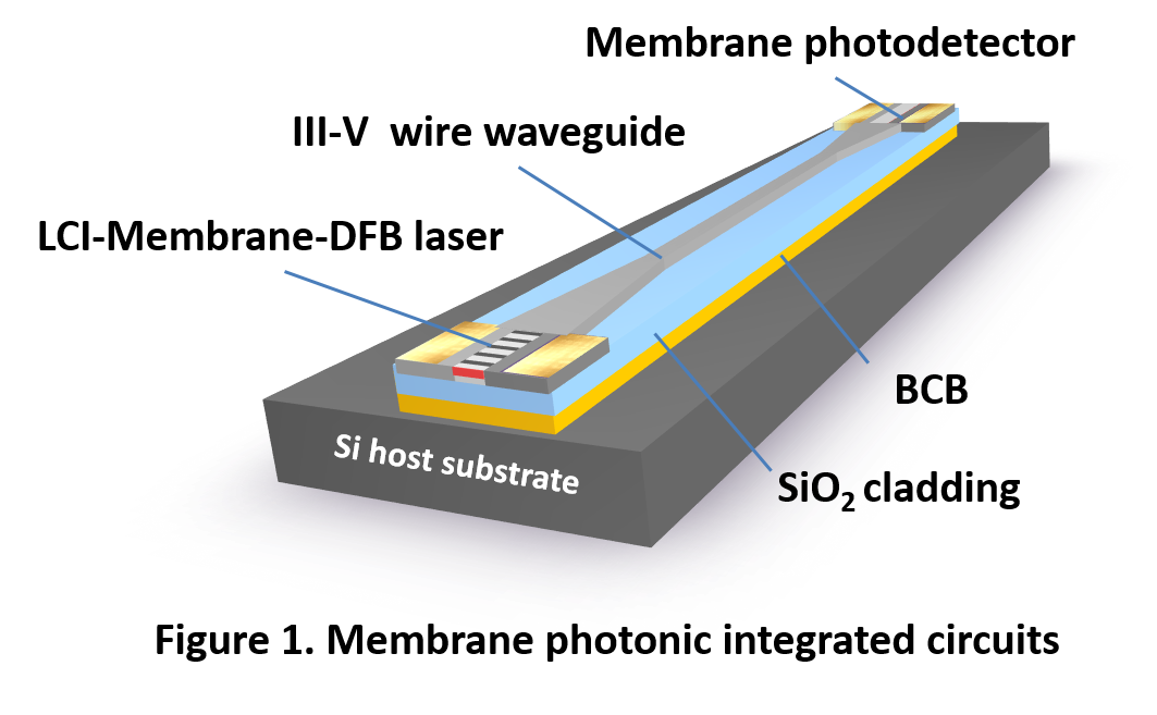
■メンブレン集積光回路
-メンブレンDFBレーザ
-メンブレン導波路
|
| |
| 研究内容 |
| メンブレンDFBレーザ |
| 一般に使用されている半導体レーザなどの半導体デバイスには、二重ヘテロ接合と呼ばれる構造が利用されています。これは屈折率が高く光が閉じ込まりやすいコア層の上下を、 コア層よりも屈折率の低い材料を用いた層(クラッド層)で覆う形にすることで、 発生した光がコア層とクラッド層の境界で全反射し、効率よく光が増幅される構造です。 しかしこの構造ではコアとクラッドに類似の半導体材料を用いていているため、 コア-クラッド間の屈折率差は非常に小さいものとなり(5%程度)、 そのためコア内への光閉じ込め効果も弱いものでした(量子井戸1層あたり1%程度)。 本研究室ではクラッド層にベンゾシクロブテン(BCB)などの屈折率が比較的低い(BCBの屈折率は約1.5、InP系材料の屈折率は3以上)の透明誘電体を用いることにより、 光閉じ込めを従来の3倍以上にまで高めることのできる「半導体薄膜構造」を提案し以下に示す研究を進めています。
|
|
| |
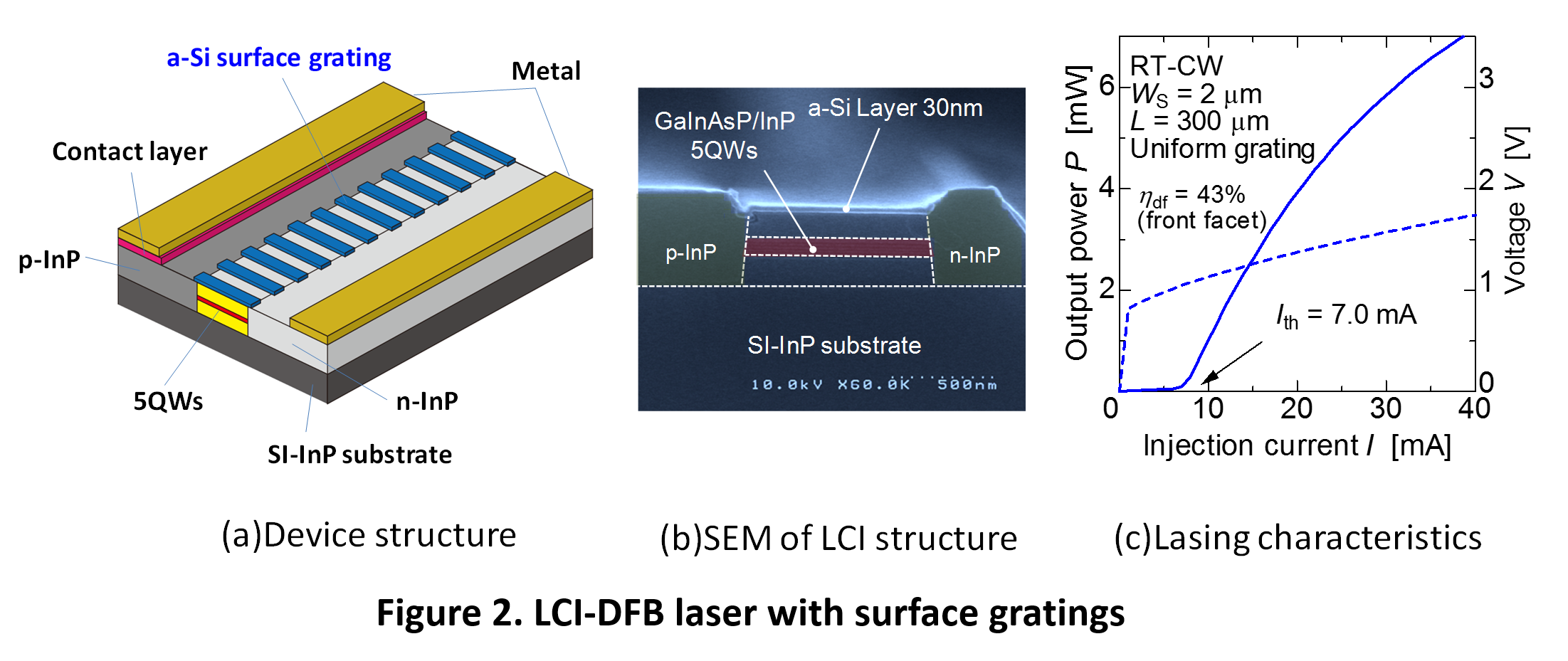
| 1) 電流注入動作の実現
|
| |
|
| |
| 半導体薄膜レーザではこれまでに、光励起下において低しきい値動作が実証されていますが、 外部励起光が不要な電流注入動作の実現が重要な課題となります。 半導体薄膜レーザの電流注入動作に向けて、pn接合をクラッド層の上下ではなく、左右に形成しキャリヤ注入を行う横方向電流注入構造(LCI = Lateral Current Injection)を導入しております。このLCI構造での動作を確認するために、半絶縁性基板上LCI構造を作製し、電流注入動作を達成しています。この構造は下部クラッド層が半導体材料であるために強光閉じ込め効果は得られませんが、 薄膜コア層を有するLCIレーザが実現可能であることを示しています。さらにFigure 2に示すようにLCI構造に表面回折格子を形成したLCI-DFBレーザでは従来型の半導体レーザと比較しても遜色のない良好な発振特性が実現されています。本構造に誘電体クラッド層を導入することで、 さらなる低消費電力動作が期待できる電流注入型半導体薄膜レーザを実現します。
|
| |
| 2) 横方向電流注入型半導体薄膜レーザ
|
| |
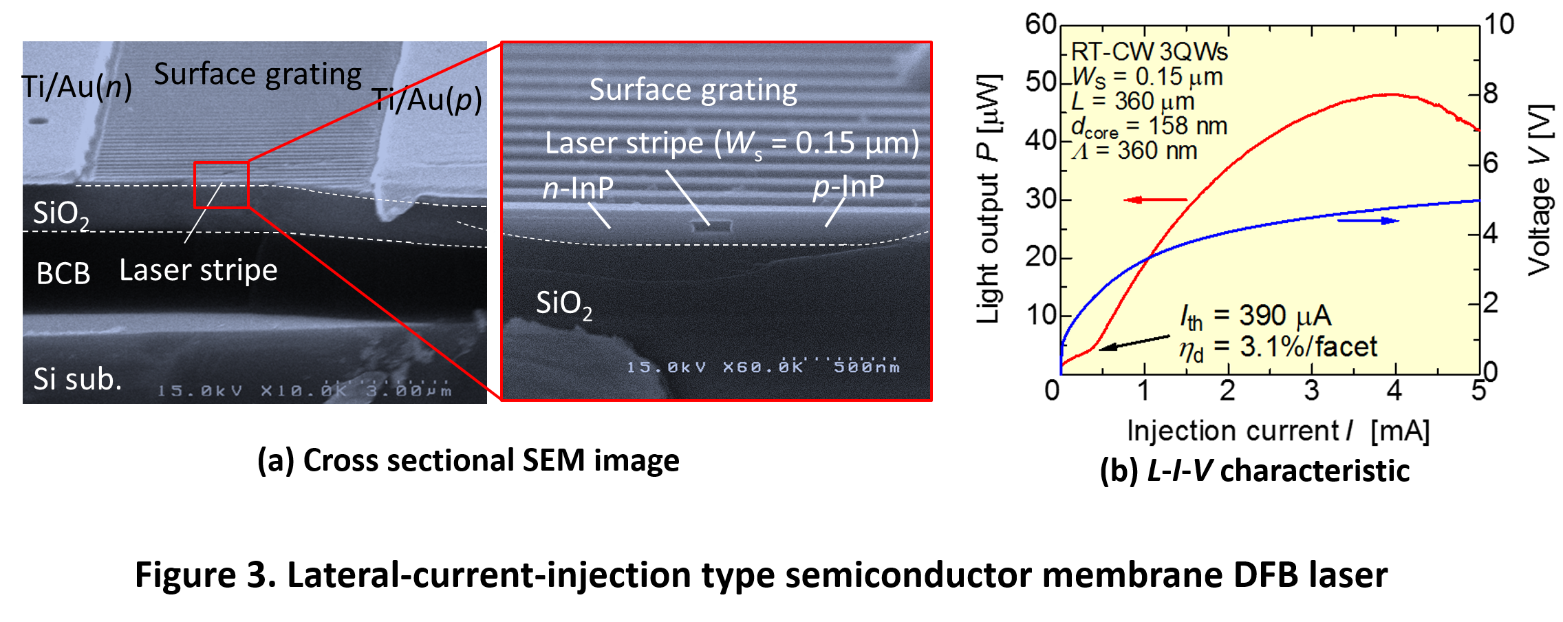 |
| 電流注入型の半導体薄膜レーザについては、レーザ活性層を有する薄膜コア層をどのように形成するかが課題となります。上で述べたLCI構造を導入した半導体薄膜レーザの実現に向けて、BCB貼り付けによる薄膜構造の形成を採用しています。これまでに、半導体薄膜ファブリペローレーザにおける室温連続動作を実現してきていましたが、最近では半導体薄膜DFBレーザにおいてFigure 3に示すようにしきい値電流1 mA以下での室温連続動作を達成しております。今後チップ上への応用に向けて、一桁以上のしきい値電流の低減が求められ、さらに強結合な共振器の導入が必要となります。 |
| |
| 3) BJB集積構造を有する横方向電流注入型半導体薄膜レーザ
|
| |
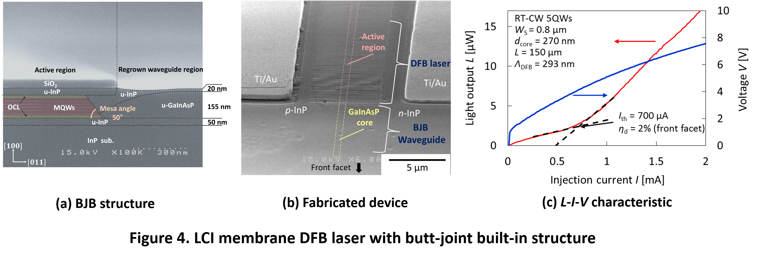 |
| LSIチップ内に薄膜レーザを導入する場合、導波路との集積構造が必要となります。この集積方法の一つとして、butt-joint built-in (BJB)構造が挙げられます。このBJB構造は能動領域と受動領域とを結晶成長を用いて接合を形成するものです。Figure4 (a)に実際のBJB構造の断面図を示しています。このように受動領域が平坦に埋め込まれている様子が確認できます。この構造を用いてFigure 4 (b)に示すような薄膜DFBレーザを作製し、しきい値電流1 mA以下での室温連続動作を達成しております。この集積構造を有する素子については従来に比べ外部微分量子効率が低く、導波路損失や散乱損失の影響が考えられ、今後改善が必要となります。
|
| △ このページのトップ △ |
| |
| |
| |
| List of reports |
| Journal Papers |
(1) T. Okamoto, N. Nunoya, Y. Onodera, S. Tamura and S.
Arai, “Continuous wave operation of optically pumped membrane
DFB laser,” Ellectron. Lett., vol. 37, no. 24, pp. 1455-1456,
Nov. 2001.
(2) T. Okamoto, N. Nunoya, Y. Onodera, S. Tamura and S. Arai,
“Single-Mode Operation of Optically Pumped Membrane Buried
Heterostructure Distributed-Feedback Lasers,” Jpn. J. Appl.
Phys., vol. 41, no. 3A, pp. L249-L251, Mar. 2002.
(3) T. Okamoto, N. Nunoya, Y. Onodera, S. Tamura and S. Arai,
“Low-Threshold Singlemode Operation of Membrane BH-DFB Lasers,”
Ellectron. Lett., vol. 38, no. 23, pp. 1444-1446, Nov. 2002.
(4) T. Okamoto, N. Nunoya, Y. Onodera, T. Yamazaki, S. Tamura
and S. Arai, “Optically Pumped Membrane BH-DFB Lasers for
Low-Threshold and Single-Mode Operation,” IEEE J. Select.
Topics in Quantum Electron., vol. 9, no. 5, pp. 1361-1366,
Sept. /Oct. 2003.
(5) T. Okamoto, T. Yamazaki, S. Sakamoto, S. Tamura and S.
Arai, “Low Threshold Membrane BH-DFB Laser Arrays with Precisely
Controlled Wavelength over a Wide Range,” IEEE Photon. Technol.
Lett., vol. 15, no. 5, pp. 1242-1244, May 2004.
(6) S. Sakamoto, T. Okamoto, T. Yamazaki, S. Tamura and S.
Arai, “Multiple-Wavelengths Membrane BH-DFB Laser Arrays,”
IEEE J. Select. Topics in Quantum Electronics, No. 11, Vol.
5, pp. 1174-1179, Sep. /Oct. 2005.
(7) S. Sakamoto, H. Naitoh, M. Ohtake, Y. Nishimoto, T. Maruyama, N. Nishiyama, and S. Arai, “85°C Continuous-Wave Operation of GaInAsP/InP-Membrane Buried Heterostructure Distributed Feedback Lasers with Polymer Cladding Layer,” Jpn. J. Appl. Phys., vol. 46, no. 47, pp. 1155-1157, Nov. 2007
(8) H. Naitoh, S. Sakamoto, Mamoru Otake, T. Okumura, T. Maruyama, N. Nishiyama, and S. Arai, “GaInAsP/InP Membrane Buried Heterostructure Distributed Feedback Laser with Air-Bridge Structure,” Jpn. J. Appl. Phys., vol. 46, no. 47, pp. 1158-1160, Nov. 2007.
5, pp. 1174-1179, Sep. /Oct. 2005.
(9) S. Sakamoto, Y. Nishimoto, S. Tamura, T. Maruyama, N. Nishiyama, and S. Arai, “Strongly Index-Coupled Membrane BH-DFB Lasers With Surface Corrugation Grating,” IEEE J. Select. Top. in Quantum Electron., vol. 13, no. 5, pp. 1135-1141, Sep. 2007.
(10) T. Okumura, M. Kurokawa, M. Shirao, D. Kondo, H. Ito, N. Nishiyama, T. Maruyama, and S. Arai, “Lateral current injection GaInAsP/InP laser on semi-insulating substrate for membrane-based photonic circuits,” Opt. Express, Vol. 17, No. 15, pp. 12564-12570, Jul. 2009.
(11) T. Okumura, H. Ito, D. Kondo, N. Nishiyama, and S. Arai, “Continuous Wave Operation of Thin Film Lateral Current Injection Lasers Grown on Semi-insulating InP,” Jpn. J. Appl. Phys., vol. 49, no. 4, pp. 040205, Apr. 2010.
(12) S. Arai, N. Nishiyama, T. Maruyama, and T. Okumura, “GaInAsP/InP Membrane Lasers for Optical Interconnects,” IEEE J. Sel. Top. Quantum Electron., vol. 17, no. 5, pp. 1381-1389, Sep. 2011.
(13) T. Shindou, T. Okumura, H. Ito, T. Koguchi, D. Takahashi, Y. Atsumi, J. Kang, R. Osabe, T. Amemiya, N. Nishiyama, and S. Arai, “Lateral-Current-Injection Distributed Feedback Laser with Surface Grating Structure,” IEEE J. Sel. Top. Quantum Electron., vol. 17, no. 5, pp. 1175-1182, Sep. 2011.
(14) T. Okumura, D. Kondo, H. Ito, S. Lee, T. Amemiya, N. Nishiyama, and S. Arai, “Lateral Junction Waveguide-Type Photodiode Grown on Semi-Insulating InP Substrate,” Jpn. J. Appl. Phys., vol. 50, no. 2, pp. 020206-1-020206-3, Feb. 2011.
(15) T. Shindou, T. Okumura, H. Ito, T. Koguchi, D. Takahashi, Y. Atsumi, J. Kang, R. Osabe, T. Amemiya, N. Nishiyama, and S. Arai, “GaInAsP/InP lateral-current-injection distributed feedback laser with a-Si surface grating,” Opt. Express, vol. 19, no. 3, pp. 1884-1891, Jan. 2011
(16) M. Futami, T. Shindo, T. Koguchi, K. Shinno, T. Amemiya, N. Nishiyama, and S. Arai, “GaInAsP/InP Lateral Current Injection Laser with Uniformly Distributed Quantum Well Structure,” IEEE Photonics Technol. Lett., vol. 24, no. 11, pp. 888-890, Jun. 2012.
|
| |
| International Conferences |
| (1) T. Okamoto, N. Nunoya, Y. Onodera, S. Tamura and S.
Arai, “CW Operation of Optically Pumped Membrane DFB Laser,”
The 4th Pacific Rim Conf. On Lasers and Electro-Optics (CLEO/PR2001),
WJPD1-10, pp.44-45 (PD), Makuhari Chiba, Japan), July 2001.
(2) T. Okamoto, N. Nunoya, Y. Onodera, S. Tamura and S. Arai,
“Single Mode Operation of Optically Pumped Membrane BH-DFB
Lasers,” The 14th Annual Meeting of The IEEE Lasers &
Electro-Optics Society (LEOS2001), PD1.1, San Diego (USA),
Nov. 2001.
(3) T. Okamoto, N. Nunoya, Y. Onodera, S. Tamura and S. Arai,
“1550nm Wavelength Membrane DFB Laser Cladded by BCB Polymer,”
5th International Symposium on Contemporary Photonics Technology
(CPT2002), Tokyo, E-21, pp. 101-102, Jan. 2002.
(4) T. Okamoto, N. Nunoya, Y. Onodera, S. Tamura and S. Arai,
“Low threshold operation of membrane buried heterostructure
distributed feedback laser,” 14th Indium Phosphide and Related
Materials Conf. (IPRM2002), Stockholm, PI-4, pp.115-118, May,
2002.
(5) T. Okamoto, Y. Onodera, T. Yamazaki, S. Tamura and S.
Arai, “Membrane Distributed Feedback Lasers for Ultra Low
Threshold Current Operation,” The 9th Int'l Symposium on Quantum
Effect Electronics, 9, pp. 58-61, Tokyo, Nov. 2002.
(6) T. Okamoto, Y. Onodera, T. Yamazaki, S. Tamura and S.
Arai, “Low Threshold Membrane BH-DFB Laser Arrays for 1490-1565nm
Wavelength Range,” 15th Indium Phosphide and Related Materials
Conf. (IPRM2003), Santa Barbara, FA2.5, pp. 558-561, May,
2003.
(7) S. Arai, T. Okamoto, Y. Onodera, T. Yamazaki, S. Tamura,
“Low Threshold GaInAsP/InP Membrane BH-DFB Lasers,” (Invited),
The 8th Optoelectronics and Communications Conference (OECC2003),
Shanghai, Oct. 2003.
(8) T. Okamoto, T. Yamazaki, S. Sakamoto, S. Tamura and S.
Arai, “Low Threshold Operation of Optically Pumped Membrane
BH-DFB Laser Arrays with a Wide Wavelength Range,” The 16th
Annual Meeting of The IEEE Lasers & Electro-Optics Society
(LEOS2003), WT 2, pp. 636-637, Tucson (USA), Oct. 2003.
(9) T. Okamoto, T. Yamazaki, S. Sakamoto, S. Tamura and S.
Arai, “Short Cavity Membrane BH-DFB Laser with l/4
Phase Shift,” 16th Indium Phosphide and Related Materials
Conf. (IPRM2004), WA-3-3, pp. 519-523, Kagoshima, May, 2004.
(10) T. Okamoto, T. Yamazaki, S. Sakamoto, S. Tamura and S.
Arai, “Improved Temperature Insensitivity of Membrane BH-DFB
Laser with Polymer Cladding Layers”, The 9th Optoelectronics
and Communication Conference (OECC2004), 14E2-3, pp. 528-529,
Yokohama, July, 2004.
(11) T. Okamoto, T. Yamazaki, S. Sakamoto, S. Tamura and S.
Arai, “Multiple-Wavelengths Low-Threshold Membrane BH-DFB
Laser Arrays”, 2004 IEEE 19th International Semiconductor
Laser Conference, WC1, Matsue, Sept., 2004.
(12) S. Sakamoto, T. Okamoto, T. Yamazaki, H. Kawashima, Tang
Jing-Long, S. Tamura and S. Arai, “Narrow Stripe Membrane
BH-DFB Lasers for Lateral-Mode Control,” The 6th Pacific Rim
Conf. On Lasers and Electro-Optics (CLEO/PR2005), CTuJ 4-6,
Tokyo, July 2005
(13) S. Sakamoto, H. Kawashima, H. Naitoh, S. Tamura, T. Maruyama
and S. Arai, “Narrow Stripe Membrane BH-DFB Lasers with Surface
Corrugation for Stable Single-Mode Operation”, The 18th International
Conference on Indium Phosphide and Related Materials (IPRM2006),
TuA1-7, Princeton, USA, May 2006.
(14) S. Sakamoto, H. Kawashima, H. Naitoh, S. Tamura, T. Maruyama
and S. Arai, “Narrow Stripe Membrane BH-DFB Lasers with Surface
Corrugation for Stable Single-Mode Operation”, The 11th International
Conference on Optical Electrical Comunication Conference (OECC2006),5E1-3,
Kaohsiung, Taiwan, July 2006.
(15) S. Sakamoto, H. Naitoh, H. Kawashima, Y. Nishimoto, S.
Tamura, T. Maruyama and S. Arai, “1-step OMVPE Grown Strongly
Index-Coupled Membrane DFB Laser with Surface Corrugation
Grating Structure,” 2006 IEEE 19th International Semiconductor
Laser Conference (ISLC2006),P 10, Hawai, USA, Sep. 2006.
(16) H. Naitoh, S. Sakamoto, M. Otake, T. Okumura, T. Maruyama, N. Nishiyama, and S. Arai, “80 oC CW Operation of GaInAsP/InP Membrane BH-DFB Laser With Air-Bridge Structure,” The 19th Indium Phosphide and Related Material (IPRM 2007), Matsue (Japan), ThB1-2, May. 2007.
(17) S. Sakamoto, H. Naitoh, H. Kawashima, M. Ohtake, S. Tamura, T. Maruyama, N. Nishiyama, and S. Arai, “85℃ continuous wave operation of membrane BH-DFB Laser cladded by benzocyclobutene,” 10th International Symposium on Contemporary Photonics Technology (CPT 2007), Tokyo (Japan), G-6, Jan. 2007.
(18) T. Okumura, M. Kurokawa, M. Shirao, D. Kondo, N. Nishiyama, and S. Arai, “Top-Air-Cladding GaInAsP/InP Lateral Current Injection Type Lasers,” IEEE Nanotechnology Materials and Device Conference 2008, MoC I-5, Oct. 2008.
(19) T. Okumura, M. Kurokawa, M. Shirao, D. Kondo, H. Ito, N. Nishiyama, and S. Arai, “GaInAsP/InP Lateral Current Injection Laser Grown on SI-InP Substrate,” 2008 International Nano-Optoelectronics Workshop, session3-P27, Aug. 2008.
(20) H. Ito, T. Okumura, D. Kondo, N. Nishiyama, and S. Arai, “Improved Quantum Efficiency of Lateral Current Injection Type Fabry-Perot Lasers,” International Symposium on Quantum Nanophotonics and Nanoelectronics, University of Tokyo, ThC-4, Nov. 2009.
(21) T. Okumura, M. Kurokawa, D. kondo, H. Ito, N. Nishiyama, and S. Arai, “Lateral Current Injection Type GaInAsP/InP DFB Lasers on SI-InP Substrate,” The 21st International Conference on Indium Phosphide and Related Materials (IPRM2009), Newport Beach, California, TuB2, May. 2009.
(22) T. Okumura, M. Kurokawa, H. Ito, D. kondo, N. Nishiyama, and S. Arai, “Room-Temperature CW Operation of Lateral Current Injection Lasers with Thin Film Lateral,” The 21st International Conference on Indium Phosphide and Related Materials (IPRM2009), Newport Beach, California, WP 12, May. 2009.
(23) T. Shindou, T. Okumura, H. Ito, T. Koguchi, D. Takahashi, Y. Atsumi, J. Kang, R. Osabe, N. Nishiyama, and S. Arai, “Lateral Current Injection Type GaInAsP/InP DFB Laser with a-Si Surface Grating,” The 23rd Annual Meeting of the IEEE Photonics Society, Denver, USA, ThR 4, Nov. 2010.
(24) . Okumura, T. Koguchi, H. Ito, N. Nishiyama, S. Arai, “First Lasing Operation of Injection Type Membrane GaInAsP DFB Laser With Lateral Current Injection BH Structure,” the 22nd IEEE International Semiconductor Laser Conference, Kyoto, Japan, ThB-2, Sep. 2010
(25) H. Ito, T. Okumura, D. kondo, N. Nishiyama, and S. Arai, “Thin-Film GaInAsP/InP Lateral Current Injection Type Fabry-Perot Laser Improved Quantum Efficiency Operation,” The 22th International Conference on Indium Phosphide and Related Materials (IPRM2010), Takamatsu, Japan, TuA3-5, Jun. 2010.
(26) D. Kondo, T. Okumura, H. Ito, S. Lee, T. Amemiya, N. Nishiyama, and S. Arai, “Lateral Junction Waveguide Type Photodiode for Membrane Photonic Circuits,” International Conference on Indium Phosphide and Related Materials, The 22nd International Conference on Indium Phosphide and Related Materials (IPRM2010), May. 2010.
(27) T. Okumura, D. Kondo, H. Ito, S. Lee, D. Takahashi, N. Nishiyama, and S. Arai, “Dynamic Characteristics of Lateral Current Injection Laser,” The 37th International Symposium on Compound Semiconductors (ISCS 2010), Kagawa, Japan, WeE3-2, May. 2010.
(29) S. Arai, N. Nishiyama, T. Okumura, “Membrane DFB Laser on SOI,” Asia Communications and Photonics Conference and Exhibition 2010 (ACP2010), Shanghai, China, ThF1, Dec. 2010.
(30) S. Arai, and N. Nishiyama, “Membrane-Type Photonic Devices for Optical Circuits on SOI,” 2010 Sokid State Devices and Materials, D-6-1, Sep. 2010.
(31) N. Nishiyama, and S. Arai, “Membrane InP-based Lasers and Related Devices for On-chip Interconnects,” IEEE Photonics Photonics 2011, WA3, Nov. 2011.
(32) T. Shindo, M. Futami, R. Osabe, T. Koguchi, T. Amemiya, N. Nishiyama, and S. Arai, “Lateral Current Injection Laser with Uniformly Distributed Quantum-Well Structure,” 2011 IEEE Photonics Conference (IPC-2011), ThC3, Oct. 2011.
(33) M. Futami, T. Shindo, T. Okumura, R. Osabe, D. Takahashi, T. Koguchi, T. Amemiya, N. Nishiyama, and S. Arai, “Stripe Width Dependence of Internal Quantum Efficiency and Carrier Injection Delay in Lateral Current Injection GaInAsP/InP Lasers,” The 16th Opto-Electronics and Communication Conference (OECC-2011), 7D2-2, Jul. 2011.
(34) T. Shindo, M. Futami, T. Okumura, R. Osabe, T. Koguchi, T. Amemiya, N. Nishiyama, and S. Arai, “Lasing Operation of Lateral-Current-Injection Membrane DFB Laser with Surface Grating,” The 16th Opto-Electronics and Communication Conference, 6D3-7, Jul. 2011.
(35) T. Shindo, T. Okumura, M. Futami, R. Osabe, T. Koguchi, T. Amemiya, N. Nishiyama, and S. Arai, “Lateral Current Injection Distributed Feedback Laser with Wirelike Active Regions,” The 23rd International Conference on Indium Phosphide and Related Materials (IPRM-2011), Tu5.2-3, May. 2011
(36) S. Arai, N. Nishiyama, T. Okumura, and T. Shindou. “Lateral current injection GaInAsP/InP laser for membrane based photonic circuits,” SPIE Photonics West Conference 2011, San Francisco, California, (USA), 7953-06, Jan. 2011.
(37) T. Shindo, M. Futami, K. Doi, T. Amemiya, N. Nishiyama, and S. Arai, “Modulation Bandwidth of GaInAsP/InP Lateral-Current-Injection Membrane Laser,” 23rd IEEE International Semiconductor Laser Conference (ISLC 2012), TuP17, Oct. 2012.
(38) K. Doi, T. Shindou, M. Futami, T. Amemiya, N. Nishiyama, and S. Arai, “Thermal Analysis of Self-Heating Effect in GaInAsP/InP Membrane DFB Laser on Si Substrate,” 2012 IEEE Photonics Conference (IPC-2012), ThO2, Sep. 2012.
(39) M. Futami, T. Shindo, K. Doi, T. Amemiya, N. Nishiyama, and S. Arai, “Low-Threshold Operation of LCI-Membrane-DFB Lasers with Be-doped GaInAs Contact Layer,” 24th International Conference on Indium Phosphide and Related Materials (IPRM 2012), Th-2C.5, Aug. 2012.
(40) T. Shindo, T. Koguchi, M. Futami, K. Shinno, K. Doi, T. Amemiya, N. Nishiyama, and S. Arai, “10 Gb/s Operation of GaInAs/InP Top Air-Clad. Lateral Junction Waveguide-type Photodiode,” 2012 IEEE Optical Interconnects Conference (OIC-2012), TuP2, May. 2012.
(41) M. Futami, K. Shinno, T. Shindo, K. Doi, T. Amemiya, N. Nishiyama, and S. Arai, “Improved Quantum Efficiency of GaInAsP/InP Top Air-Clad Lateral Current Injection Lasers,” 2012 IEEE Optical Interconnects Conference (OIC-2012), TuB3, May. 2012
|
| |
| Meeting Report |
| (1) T. Okamoto, Y. Onodera, T. Yamazaki, S. Tamura and
S. Arai, “A Study of Semiconductor Membrane BH-DFB Laser Arrays,”
「半導体薄膜BH-DFBレーザに関する研究」 Technical Report of IEICE, OPE2003-30
(2003-07), pp.35-38, Tokyo (Japan), July 2003.
(2) T. Okamoto, T. Yamazaki, S. Sakamoto, S. Tamura and S.
Arai, “Polymer Cladded Semiconductor Membrane BH-DFB Lasers,”
「誘電体クラッド半導体薄膜BH-DFBレーザ」 Technical Report of IEICE, OPE2004-20
(2004-07), pp.11-14, Tokyo (Japan), July 2004.
(3) S. Sakamoto, H. Naitoh, S. Tamura, T. Maruyama and S.
Arai, “Membrane BH-DFB Laser with Surface Corrugation Grating”,
「凹凸形状回折格子を用いた半導体薄膜BH-DFBレーザ」, Technical Report of IEICE, OPE2006-19
(2004-06), pp.1-6, Tokyo (Japan), June 2006.
|
| |
| Domestic Conferences |
| (1) K. Matsui, T. Okamoto, N. Nunoya and S. Arai, “Analysis
of threshold current of membrane DFB lasers with wirelike
active regions,” 「半導体薄膜活性層分離型DFBレーザの閾値電流解析」 Nat. Conv. Res.
of Japan Soc. Appl. Phys., 30a-ZS-7, Digest III pp. 1152,
Tokyo, Mar. 2001.
(2) T. Okamoto, N. Nunoya, Y. Onodera, S. Tamura and S. Arai,
“Room Temperature CW Operation of Optically-Pumped Membrane
DFB Lasers,” 「半導体薄膜構造DFBレーザの光励 起室温連続動作」 Nat. Conv. Res. of
Japan Soc. Appl. Phys., 13p-B-14, Digest III pp. 869, Aichi,
Sep. 2001.
(3) T. Okamoto, N. Nunoya, Y. Onodera, S. Tamura and S. Arai,
“Single-Mode Operation of Optically Pumped Membrane BH-DFB
Lasers,” 「BH構造を導入した光励起半導体薄膜DFBレーザの単一モード動作」 Nat. Conv. Res.
of Japan Soc. Appl. Phys., 29a-YS-9, Digest III pp. 1144,
Kanagawa, Mar. 2002.
(4) Y. Onodera, T. Okamoto, N. Nunoya, S. Tamura and S. Arai,
“Low Threshold Operation of Membrane BH-DFB Lasers,” 「半導体薄膜DFBレーザの低しきい値動作」
Nat. Conv. Res. of Japan Soc. Appl. Phys., 29a-YS-9, Digest
III pp. 1144, Kanagawa, Mar. 2002.
(5) T. Okamoto, Y. Onodera, T. Yamazaki, S. Tamura and S.
Arai, “Proposal of Multiple Wavelength Membrane DFB Laser
Array,” 「位相シフト変調型半導体薄膜DFB多波長アレイ光源の提案」Nat. Conv. Res. of Japan
Soc. Appl. Phys., 26p-A-12, Digest III pp. 996, Niigata, Sep.
2002.
(6) T. Okamoto, Y. Onodera, T. Yamazaki, S. Tamura and S.
Arai, “Wavelength Controllability of Membrane BH-DFB Lasers,”
「半導体薄膜BH-DFBレーザの波長制御性」 Nat. Conv. Res. of Japan Soc. Appl.
Phys., 28p-ZQ-16, Digest III pp. 1241, Kanagawa, Mar. 2003.
(7) T. Okamoto, Y. Onodera, T. Yamazaki, S. Tamura and S.
Arai, “Fabrication of Multiple Wavelength Membrane BH-DFB
Laser Arrays,” 「半導体薄膜BH-DFB多波長レーザアレイの試作」Nat. Conv. Res. of
Japan Soc. Appl. Phys., 28p-ZQ-17, Digest III pp. 1241, Kanagawa,
Mar. 2003.
(8) T. Okamoto, T. Yamazaki, S. Tamura and S. Arai, “Room
Temperature CW Operation of Phase Shifted Membrane BH-DFB
Laser,” 「位相シフト半導体薄膜BH-DFBレーザの室温連続動作」Nat. Conv. Res. of Japan
Soc. Appl. Phys., 30p-YB-11, Digest III pp. 1041, Fukuoka,
Aug. 2003.
(9) T. Yamazaki, T. Okamoto, S. Tamura and S. Arai, “Low Threshold
Operation of Membrane BH-DFB Laser Arrays,” 「半導体薄膜BH-DFBレーザアレイの低しきい値動作」
Nat. Conv. Res. of Japan Soc. Appl. Phys., 30p-YB-12, Digest
III pp. 1042, Fukuoka, Aug. 2003.
(10) T. Okamoto, T. Yamazaki, S. Sakamoto, S. Tamura and S.
Arai, “Athermal effect of polymer cladded membrane BH-DFB
laser,” 「誘電体クラッドを用いた半導体薄膜BH-DFBレーザにおけるアサーマル効果の観測」Nat. Conv.
Res. of Japan Soc. Appl. Phys., 30a-ZZ-5, Digest III pp. 1260,
Tokyo, Mar. 2004.
(11) T. Yamazaki, T. Okamoto, S. Sakamoto, S. Tamura and S.
Arai, “Multiple wavelength membrane BH-DFB laser arrays,”
「一括励起半導体薄膜BH-DFB多波長レーザアレイの試作」Nat. Conv. Res. of Japan Soc.
Appl. Phys., 30a-ZZ-6, Digest III pp. 1260, Tokyo, Mar. 2004.
(12) S. Sakamoto, T. Okamoto, T. Yamazaki, S. Tamura and S.
Arai, “Athermal effect of polymer cladded membrane BH-DFB
laser,” 「誘電体クラッドを用いた半導体薄膜BH-DFBレーザにおけるアサーマル効果の観測」Nat. Conv.
Res. of Japan Soc. Appl. Phys., 1a-ZN-9, Digest III Miyagi,
Sept. 2004.
(13) T. Okamoto, S. Sakamoto, T. Yamazaki, S. Tamura and S.
Arai, “Membrane BH-DFB laser array with exposure control,”
「EB露光量制御による微小波長間隔半導体薄膜BH-DFBレーザアレイ」Nat. Conv. Res. of Japan
Soc. Appl. Phys., 1a-ZN-10, Digest III Miyagi, Sept. 2004.
(14) T. Okamoto, S. Sakamoto, T. Yamazaki, S. Tamura and S.
Arai, “Membrane BH-DFB Laser with High Index Difference Waveguide”,
「高屈折率差導波路構造を用いた半導体薄膜BH-DFBレーザ」, The 65th Autumn Meeting, 2004;
The Japan Society of Applied Physics., 1a-ZN-10, Digest III
-p. 1020, Sendai, Sep. 2004.
(15) S. Sakamoto, T. Okamoto, T. Yamazaki, H. Kawashima, Tang
Jing-Long, S. Tamura and S. Arai, “Membrane BH-DFB Laser Array
with Asperity Corrugation Structure”, 「凹凸形状回折格子を用いた半導体薄膜BH-DFBレーザアレイ」,
The 52nd Spring Meeting, 2005; The Japan Society of Applied
Physics and Related Societies., 31p-ZH-5, Saitama, Mar./Apr.
2005.
(16) H. Kawashima, S. Sakamoto, T. Okamoto, T. Yamazaki, Tang
Jing-Long, S. Tamura and S. Arai, “Lateral-Mode Control of
Membrane BH-DFB Lasers with Narrow Stripe”, 「狭ストライプ半導体薄膜BH-DFBレーザの横モード制御」,
The 52nd Spring Meeting, 2005; The Japan Society of Applied
Physics and Related Societies.,31p-ZH-6, Saitama, Mar./Apr.
2005.
(17)S. Sakamoto, H. Kawashima, H. Naitoh, S. Tamura, T. Maruyama,
and S. Arai, “Narrow Stripe Membrane BH-DFB Laser Array using
Surface Corrugation”「凹凸形状回折格子を用いた狭ストライプ半導体薄膜BH-DFBレーザアレイ」,
The 53rd Spring Meeting, 2006; The Japan Society of Applied
Physics and Related Societies.,23a-Za-4, Tokyo, Mar. 2006.
(18)S. Sakamoto, H. Naitoh, H. Kawashima, Y. Nishimoto, S.
Tamura, T. Maruyama, and S. Arai, “High Temperature Continuous
Wave Operation of Membrane BH-DFB Laser”「 半導体薄膜BH-DFBレーザの高温連続動作」,
The 67th Autumn Meeting, 2006; The Japan Society of Applied
Physics., 29a-ZT-5, Digest III pp.1046 , Shiga, Aug. 2006.
(19)S. Sakamoto, H. Naitoh, H. Kawashima, S. Tamura, T. Maruyama,
and S. Arai, “Low Threshold Operation of Short Cavity Membrane
BH-DFB Laser using Surface Corrugation Grating”「凹凸形状回折格子を用いた短共振器半導体薄膜BH-DFBレーザの低しきい値動作」,
The 67th Autumn Meeting, 2006; The Japan Society of Applied
Physics., 29a-ZT-6, Digest III pp.1046 , Shiga, Aug. 2006.
(20)H. Naitoh, S. Sakamoto, H. Kawashima, Y. Nishimoto, S.
Tamura, T. Maruyama, and S. Arai, “1-step OMVPE Grown Index
Coupled Membrane DFB Laser with Surface Corrugation Structure,”「1回OMVPE成長による凹凸形状半導体薄膜DFBレーザ」,
The 67th Autumn Meeting, 2006; The Japan Society of Applied
Physics., 29a-ZT-7, Digest III pp.1047 , Shiga, Aug. 2006.
|
| |
| Awards |
(1) T. Okamoto, “Continuous Wave Operation of Optically Pumped
Membrane DFB Laser,” Student Paper Contest, Third Place, IEEE
Student Branch at Tokyo Institute of Technology, Dec. 2001.
(2) T. Okamoto, “Membrane Distributed Feedback Lasers for Ultra
Low Threshold Current Operation,” Student Paper Contest, Third
Place, IEEE Student Branch at Tokyo Institute of Technology,
Dec. 2002.
(3) T. Okamoto, “Low Threshold and Precisely Wavelength Controlled
Membrane BH-DFB Laser Arrays with a Wide Wavelength Range,”
Student Paper Contest, First Place, IEEE Student Branch at Tokyo
Institute of Technology, Dec. 2003.
(4) 岡本健志 「位相シフト半導体薄膜BH-DFBレーザの室温連続動作」 第15回応用物理学会講演奨励賞2004年3月.
(5) 黒川宗高 「OMVPE再成長法による薄膜クラッド層を有する横方向電流注入型レーザ」 第25回応用物理学会講演奨励賞2008年9月
|
| |
| △ このページのトップ △ |
| |
| |
| |
| 研究内容 |
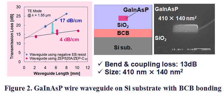
| 半導体メンブレン導波路 |
| Si基板上Ⅲ-Ⅴ族メンブレン光回路の実現のためには、半導体メンブレンレーザからの光信号をより低損失に伝送できる光導波路配線が必要になります。 本研究室では、光信号伝送に必要な導波路に関して、Si電子回路上にバックエンドプロセスで集積可能かつ低消費電力・小型光回路が実現可能という利点から、III-V族半導体を低屈折率材料で挟んだメンブレン構造を利用したメンブレンレーザとの集積を提案しております。そして、実際にモノリシック集積を目的としたIII-V族化合物半導体材料を用いた導波路として、「BCB貼り付けによるSi基板上メンブレンGaInAsP導波路」の研究を行っています。
|
| |
| 1) BCB貼付
|
| |

|
| |
| 図1はBCBを用いた貼付プロセスを示しております。OMVPE法を用いてInP基板上にInPバッファー層、 エッチストップ層 (GaInAs / InP)、GaInAsPコア層、最後に、InPキャップ層を成長し、この成長基板からInPキャップ層を除去し、P-CVDを用いて導波路の下部クラッドになるSiO2を堆積します。その後、Si基板上に粘着性のあるBCBをスピンコートし、BCB中の溶媒の一部を蒸発させ、約80%固形化します。次に、それらの両基板を貼り付け、その後、BCBを完全に固形化します。 貼り付けの最終プロセスとして、選択エッチングを用いて、InP基板、GaInAsエッチストップ層及び、InPエッチストップ層を除去し、メンブレン化します。
|
| |
| 2) GaInAsP細線導波路
|
| |
|
| |
| GaInAsP細線導波路については、伝播損失 4dB/cmの低損失導波路が得られております。今後Si基板上Ⅲ-Ⅴ族メンブレン光回路の実現に向けて、より低損失導波路を目指し、レーザとの集積及びGaInAsP導波路デバイスとしての光機能素子への研究が進められております。
|
| |
| List of reports |
| Journal Papers |
(1) J. Lee, Y. Maeda, Y. Atsumi, Y. Takino, N. Nishiyama, and S. Arai, “Low-loss GaInAsP wire waveguide on Si substrate with Benzocyclobutene adhesive wafer bonding for membrane photonic circuits,” Jpn. J. App. Phys., Vol. 51, pp. 042201-1 ? 042201-5, Apr. 2012.
|
| |
| International Conferences |
| (1) Y. Maeda, J. Lee, Y. Atsumi, N. Nishiyama, and S. Arai, “Uniform BCB bonding process toward low propagation loss in GaInAsP photonic wire waveguide on Si wafer,” The 23rd Indium Phosphide and Related Materials (IPRM 2011), Berlin (Germany), P08, May 2011.
(2) Lee, Y. Yamahara, Y. Atsumi, T. Shindo, N. Nishiyama, and S. Arai, “Compact InP-based 1×2 MMI Splitter on Si Substrate with BCB Bonding for Membrane Photonic Circuits,” 24th Indium Phosphide and Related Materials (IPRM2012), Santa Barbara (USA), Mo.1C1, Aug. 2012.
|
| |
| Domestic Conferences |
| (1) Y. Maeda, Y. Atsumi, N. Nishiyama, and S. Arai, “Ⅲ-Ⅴ族薄膜光回路実現のためのSi基板上BCB貼り付けGaInAsP薄膜構造品質の改善,” The 71st Autumn Meeting; The Japan Society of Applied Physics, 14p-G-14, Aug. 2010.
(2) J. Lee, Y. Maeda, Y. Atsumi, Y. Takino, N. Nishiyama, and S. Arai, “BCB貼り付けを用いたSi基板上低損失GaInAsP細線導波路の実現,” The 72nd Autumn Meeting, The Japan Society of Applied Physics and Related Societies, 31p-ZN-3, Yamagata, Japan, Aug. 2011.
(3) J. Lee, Y. Yamahara, Y. Atsumi, T. Shindo, N. Nishiyama, and S. Arai, “BCB貼り付け法によるSi基板上GaInAsP細線1×2 MMIの作製,” The 59th Spring Meeting, The Japan Society of Applied Physics and Related Societies, 17a-F4-11, Tokyo, Japan, Mar. 2012.
(4) J. Lee, Y. Yamahara, T. Shindo, M. Futami, K. Doi, N. Nishiyama, and S. Arai, “InP系横接合型半導体能動薄膜光素子と細線光導波路のテーパー結合,” The 2012 IEICE Society Conf., C-3-93, Toyama, Japan, Sept. 2012.
|
| |
| △ このページのトップ △ |
|
| |
 |
|