| |
| 研究内容 |
| 量子細線レーザ |
 |
極微細構造を応用した高性能光デバイスの実現
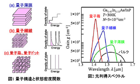
図1(a)に示す量子薄膜構造は、光通信用だけではなく、光ディスク用など、さまざまな用途の半導体レーザに応用されてきました。そして、図1(b)、ならびに図1(c)に示すように量子構造が量子細線、さらには量子箱と低次元化する、つまり、キャリアの自由度の次元が減ると、図1に示すように状態密度関数が先鋭化していきます。そして、これに起因して、図2に示すように量子細線・量子箱構造では光利得のピーク値が高くなります。その結果、量子細線・量子箱構造を活性層にもつ半導体レーザでは、低消費電力及び高効率、さらには変調速度やスペクトル線幅などの特性も飛躍的に向上させることができます。
これまでに、エッチングによる極微細構造の形成、量子ドット構造の作製法として広く用いられている自己組織化成長法、パターン基板や傾斜基板上への選択成長法を用いて、量子細線・量子箱レーザの研究が行なわれてきました。我々は、他の作製法と比べて、任意極微形状を形成できる点及び活性層の周期的配置による分布帰還
(DFB) レーザへの応用の観点で有利と考えられる電子ビーム露光・ドライエッチング・有機金属気相成長法による埋め込み再成長を用いて、量子細線・量子箱レーザの作製を行なってきました。そして、世界最高水準の極微細加工技術を用いることにより、低損傷極微細構造の形成、さらにはドライエッチング及び再成長法を用いた量子細線レーザとして、初めて室温連続動作を実現すると共に、その寿命測定を行った結果、12,000時間以上経過後においても良好な特性を維持していることを確認し、この作製法が実用デバイスの作製に適用可能であることを明らかにしてきました。 |
| |
(I) 歪補償量子細線レーザ
これまでに、電子ビーム露光法・CH4/H2反応性イオンエッチング・2段階有機金属気相成長法を用いたいわゆるトップダウン的作製法により実現された量子細線レーザ(活性層幅23nm、5層量子細線構造)として世界で初めて室温連続発振を実現しております。また、その寿命測定を行った結果、12,000時間以上経過後においても良好な特性を維持していることを確認しております。また、本作製法により形成された多層量子細線構造がサイズ均一性に優れていること(細線幅の標準偏差±2nm以下)も明らかに致しております。
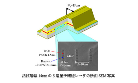
さらに、狭細線構造 (活性層幅14nm)を有する5層量子細線レーザを実現し、自然放出光スペクトルの測定と理論解析との比較から、高エネルギー側における量子薄膜レーザよりも急峻なスペクトル形状は、キャリヤの横方向量子閉じ込め効果に起因していることを明らかに致しております。
今後、サイズ及び各量子井戸層の組成・層厚分布を低減することによる狭利得スペクトル特性の実現、ならびに高反射率反射鏡とDFB構造の付加により低電流・高効率動作の実現を目指します。
|
 |
| |
(II) 機能光デバイスのための新しい極微構造の探索
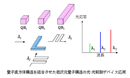
量子閉じ込め効果が顕著な量子細線構造では、細線に平行な方向の電界成分を有する双極子モーメントが強くなります。さらに、その細線幅を変えることにより、偏波異方性を有した状態で発光・吸収に寄与するエネルギー準位を変えることができます。そこで、線幅及び長さの異なる量子直方体構造を結合させた低次元量子構造のデバイス応用の可能性を理論・実験両面から研究を行います。一例として、下図に示すような量子直方体構造をL字型、あるいはT字型に結合させた低次元量子構造を作製し、制御光と信号光を異なる偏波方向、あるいは異なる入射方向とする光-光制御デバイス及び波長変換レーザへの可能性を探索します。 |
 |
| |
| List of Reports |
| Journal Papers |
1. N. Nunoya, M. Nakamura, H. Yasumoto, S. Tamura and S. Arai,
“GaInAsP/InP Multiple-Layered Quantum-Wire Lasers Fabricated
by CH4/H2 Reactive-Ion-Etching,” Jpn. J. Appl. Phys., vol. 39,
no. 6A, pp.3410-3415, 2000.
2. N. Nunoya, H. Yasumoto, H. Midorikawa, S. Tamura and S. Arai,
“Low Threshold Current Density Operation of GaInAsP/InP Lasers
with Strain-Compensated Multiple-Layered Wirelike Active Regions,”
Jpn. J. Appl. Phys., vol. 39, no. 10B, pp. L1042-L1045, 2000.
3. H. Yagi, K. Muranushi, N. Nunoya, T. Sano, S. Tamura and
S. Arai, “GaInAsP/InP Strain-Compensated Quantum-Wire Lasers
Fabricated by CH4/H2 Dry Etching and Organometallic Vapor-Phase-Epitaxial
Regrowth,” Jpn. J. Appl. Phys., vol.
41, no. 2B, pp. L186-L189, Feb. 2002.
4. H. Yagi, K. Muranushi, N. Nunoya, T. Sano, S. Tamura and
S. Arai, “Low-Damage Etched/Regrown Interface of Strain-Compensated
GaInAsP/InP Quantum-Wire Laser Fabricated by CH4/H2 Dry Etching
and Regrowth,” Appl. Phys. Lett., , vol. 81, no. 6, pp. 966-968,
Aug. 2002.
5. T. Sano, H. Yagi, K. Muranushi, S. Tamura, T. Maruyama, A.
Haque and S. Arai, “Multiple-Quantum-Wire Structures with Good
Size Uniformity Fabricated by CH4/H2 Dry Etching and Organometallic
Vapor-Phase-Epitaxial Regrowth,” Jpn. J. Appl. Phys., vol. 42,
part 1, no. 6A, pp. 3471-3472, Jun. 2003.
6. H. Yagi, T. Sano, K. Ohira, T. Maruyama, A. Haque and S.
Arai, “Room Temperature-Continuous Wave Operation of GaInAsP/InP
Multiple-Quantum-Wire Lasers by Dry Etching and Regrowth Method,”
Jpn. J. Appl. Phys., vol. 42, part 2, no. 7A, pp. L748-L750,
Jul. 2003.
7. A. Haque, H. Yagi, T. Sano, T. Maruyama and S. Arai, “Electronic
band structures of GaInAsP/InP vertically stacked multiple quantum
wires with strain-compensating barriers,” J. Appl. Phys., vol.
94, no. 3, pp. 2018-2023, Aug. 2003.
8. K. Ohira, T. Murayama, H. Yagi, S. Tamura and S. Arai, “Distributed
Reflector Laser Integrated with Active and Passive Grating Sections
Using Lateral Quantum Confinement Effect,” Jpn. J. Appl. Phys.,
vol. 42, part 2, no. 8A, pp. L921-L923, Aug. 2003.
9. H. Yagi, T. Sano, K. Ohira, D. Plumwongrot, T. Maruyama,
A. Haque, S. Tamura and S. Arai, “GaInAsP/InP Partially Strain-Compensated
Multiple-Quantum-Wire Lasers Fabricated by Dry Etching and Regrowth
Processes,” Jpn. J. Appl. Phys., vol. 43, no. 6A, Jun. 2004.
10. A. Haque, T. Maruyama, H. Yagi, T. Sano, D. Plumwongrot
and S. Arai, “Anomalous in-plane polarization dependence of
optical gain in compressively strained GaInAsP/InP quantum wire
lasers,” to be published in IEEE J. Quantum Electron., 2004. |
| |
| International Conferences |
| 1. S. Arai, N. Nunoya, M. Nakamura, H. Yasumoto and S.
Arai, “1.5 mm Wavelength GaInAsP/InP
Low Threshold Current Lasers by Low-Damage CH4/H2-RIE and
OMVPE Regrowth,” Int. Symposium on Ultra-Parallel Optoelectronics
(30th Precision & Intelligence Lab. Symposium), C-2, pp.27-28,
Kawasaki (Japan), Mar. 2000.
2. H. Yasumoto, N. Nunoya, H. Midorikawa, S. Tamura and S.
Arai, “1.5 mm Wavelength Strain-Compensated
GaInAsP/InP Wirelike Laser by CH4/H2 Reactive Ion Etching,”
The 12th Int. Conf. on Indium Phosphide and Related Materials
(IPRM’2000), WA3.2, pp. 498-501, Williamsburg (USA), May 2000.
3. S. Arai, “Low-Damage Fabrication of GaInAsP/InP Fine-Structures
for High Performance Lasers,” 4th International Workshop of
the Canadian - European Research Initiative on Nanostructures
(CERION), (Invited), Wurzburg Univ. (Germany), July 2000
4. S. Arai, H. Yasumoto, N. Nunoya, H. Midorikawa, and S.
Tamura, “Low-Damage GaInAsP/InP Fine Structure Lasers by CH4/H2-RIE
and OMVPE Regrowth,” Int. Symposium on Formation, Physics
and Device Application of Quantum Dot Structures (QDS’00),
Th1-13, p. 206, Sapporo (Japan), Sept. 2000.
5. H. Midorikawa, N. Nunoya, K. Muranushi, S. Tamura and S.
Arai, “Low-Damage Etched/Regrown Interfaces of GaInAsP/InP
Wirelike Laser with Strain-Compensated MQW Structure,” The
13th Int’l Conf. on Indium Phosphide and Related Materials
(IPRM’01), TuB2-2, pp. 67-70, Nara (Japan), May 2001.
6. H. Midorikawa, K. Muranushi, N. Nunoya, T. Sano, S. Tamura
and S. Arai, “1.5 mm Wavelength
GaInAsP/InP 5-Layered Quantum-Wire Lasers Fabricated by CH4/H2
Dry Etching and Regrowth,” The 14th Annual Meeting of The
IEEE Lasers & Electro-Optics Society (LEOS2001), WA-5,
pp. 407-408, San Diego (USA), Nov. 2001.
7. H. Yagi, K. Muranushi, N. Nunoya, T. Sano, N. Nunoya, S.
Tamura and S. Arai, “Large Blue Shift in GaInAsP/InP Vertically-Stacked
Multiple-Quantum-Wire-Lasers by Dry Etching and Regrowth Processes,”
The 14th Indium Phosphide and Related Materials Conference
(IPRM2002), A9-4, pp. 723-726, Stockholm (Sweden), May 2002.
8. H. Yagi, K. Muranushi, T. Sano, N. Nunoya, S. Tamura and
S. Arai, “GaInAsP/InP Multiple-Quantum-Wire Lasers by CH4/H2
Reactive Ion Etching,” 7th OptoElectronics and Communications
Conference (OECC2002), 10C3-4, pp. 158-159, Yokohama (Kanagawa,
Japan), Jul. 2002.
9. H. Yagi, T. Sano, K. Ohira, T. Maruyama, A. Haque and S.
Arai, “ RT-CW Operation of GaInAsP/InP Quantum-Wire Lasers
Fabricated by Dry Etching and Regrowth Method,” Sixth International
Symposium on Contemporary Photonics Technology (CPT 2003),
PDP-1, pp. 1 (PD), Shinagawa (Japan), Jan. 2003.
10. K. Ohira, T. Murayama, H. Yagi, S. Tamura and S. Arai,
“New Type Distributed Reflector Laser with Passive DBR Section
By Using Lateral Quantum Confinement Effect,” Sixth International
Symposium on Contemporary Photonics Technology (CPT 2003),
PDP-3, pp. 3(PD), Shinagawa (Japan), Jan. 2003.
11. K. Ohira, T. Murayama, H. Yagi, S. Tamura and S. Arai,
“Distributed Reflector Lasers Integrated with Passive Grating
Region By Using Lateral Quantum Confinement Effect,” The 15th
Indium Phosphide and Related Materials Conference (IPRM2003),
WB1.5, pp. 251-254, Santa Barbara, Cal. (USA), May 2003.
12. A. Haque, H. Yagi, T. Sano, T. Maruyama and S. Arai, “Energy-Band
Structures of GaInAsP/InP Vertically Stacked Multiple Quantum-Wire
Lasers with Strain-Compensating Barriers,” The 15th Indium
Phosphide and Related Materials Conference (IPRM2003), ThP11,
pp. 433-436, Santa Barbara, Cal. (USA), May 2003.
13. H. Yagi, T. Sano, K. Ohira, T. Maruyama, A. Haque and
S. Arai, “Over 2,000 Hours of RT-CW Operation of GaInAsP/InP
Vertically-Stacked Multiple-Quantum-Wire Laser,” The 15th
Indium Phosphide and Related Materials Conference (IPRM2003),
ThA2.5, pp. 378-379, Santa Barbara, Cal. (USA), May 2003.
14. A. Haque, T. Maruyama, H. Yagi, T. Sano and S. Arai, “In-Plane
Polarization Dependence of Gain in Strained Quantum-Wire Lasers
with Strain-Compensating Barriers,” The IEEE/LEOS International
Conference on Numerical Simulation of Semiconductor Optoelectronic
Devices (NUSOD-03), MA3, pp. 7-8, Tokyo (Japan), Oct. 2003.
15. T. Maruyama, A. Haque and S. Arai, “Polarization Anisotropy
in Strained Quantum-Wire Structures Considering The Strain
Relaxation Effect,” The 16th Annual Meeting of The IEEE Lasers
& Electro-Optics Society (LEOS 2003), MD5, pp. 43-44,
Tucson (USA), Oct. 2003.
16. K. Ohira, T. Murayama, H. Yagi, S. Tamura and S. Arai,
“A Novel Distributed Reflector Laser Consisting of Width Modulated
Wires in Active DFB and Passive DBR Sections,” The 16th Annual
Meeting of The IEEE Lasers & Electro-Optics Society (LEOS
2003), TuD5, pp. 204-205, Tucson (USA), Oct. 2003.
17. S. Arai, H. Yagi, T. Sano, K. Ohira, T. Maruyama, A. Haque,
D. Plumwongrot and S. Tamura, “GaInAsP/InP Long Wavelength
Quantum-Wire Lasers,” Pre-Conference of IEEE International
Semiconductor Laser Conference 2004 IEICE LQE/OPE Technical
Meeting, 20-B, pp.33-36, Kobe (Japan), Dec. 2003.
18. H. Yagi, T. Sano, K. Ohira, D. Plumwongrot, T. Maruyama,
A. Haque and S. Arai, “Reliable RT-CW operation of GaInAsP/InP
multiple-quantum-wire lasers fabricated by dry etching and
regrowth method,” Conference on Lasers and Electro Optics/International
Quantum Electronics Conference (CLEO/IQEC 2004), CThL4, p.
138, San Francisco, Cal. (USA), May 2004.
19. H. Yagi, T. Sano, K. Ohira, K. Miura, T. Maruyama, A.
Haque and S. Arai, “GaInAsP/InP Multiple-Quantum-Wire Lasers
with Narrow (14 nm) Quantum-Wire Structure,” The 16th Indium
Phosphide and Related Materials Conference (IPRM 2004), TuA3-4,
pp. 100-103, Kagoshima (Japan), May/Jun. 2004.
20. K. Ohira, T. Murayama, M. Hirose, H. Yagi, S. Tamura,
A. Haque and S. Arai, “Low-Threshold and High Efficiency Distributed
Reflector Laser with Wirelike Active Regions and Quantum-Wire
DBR,” The 16th Indium Phosphide and Related Materials Conference
(IPRM 2004), WA4-6, pp. 562-563, Kagoshima (Japan), May/Jun.,
2004.
21. H. Yagi, T. Sano, K. Miura, T. Maruyama, A. Haque and
S. Arai, “1.5 mm Wavelength GaInAsP/InP
Multiple-Quantum-Wire Lasers with SiO2/Semiconductor Reflector,”
The 9th Optoelectronics and Communications Conference (OECC2004),
14E1-4, pp. 522-523, Yokohama (Japan), Jul. 2004.
|
| |
| Meeting Reports |
| 1. H. Midorikawa, N. Nunoya, K. Muranushi, S. Tamura and
S. Arai, “Low Threshold Operation of 1.5 mm
Wavelength Strain-Compensated GaInAsP/InP Multiple Wirelike
Laser Fabricated by Low Damage CH4/H2 Dry Etching and Regrowth,”
「低損傷CH4/H2ドライエッチングと埋め込み再成長による1.5mm波長帯GaInAsP/InP歪補償多層細線レーザの低しきい値動作」
Technical Report of IEICE, OPE2001-33/LQE2001-32 (2001-07),
p.7-12, Tokyo (Japan), July 2001.
2. H. Midorikawa, K. Muranushi, N. Nunoya, T. Sano, S. Tamura
and S. Arai, “1.5 mm Wavelength
Strain-Compensated GaInAsP/InP 5-Layered Quantum-Wire Lasers
by Low-Damage CH4/H2 Reactive Ion Etching Process,” The 8th
Int. symposium on Quantum Effect Electronics, pp.50-53, Meguro,
Oct. 2001.
3. K. Ohira, N. Nunoya, A. Onomura, H. Yagi, S. Tamura and
S. Arai, “Distributed Reflector (DR) Laser with Wire Structure,”
「細線構造を有する分布反射型(DR)レーザ」 Technical Report of IEICE, LQE2002-16
(2002-05), pp. 61-64, Fukui (Japan), May 2002.
4. H. Yagi, K. Muranushi, T. Sano, N. Nunoya, S. Tamura and
S. Arai, “GaInAsP/InP Strain-Compensated Multiple-Quantum-Wire
Lasers Fabricated by Dry Etching and Regrowth,” 「ドライエッチングと埋め込み再成長法によるGaInAsP/InP歪補償多層量子細線レーザ」
Technical Report of IEICE, OPE2002-42/LQE2002-97 (2002-06),
p.27-30, Tokyo (Japan), Jul. 2002.
5. S. Arai, H. Yagi, K. Ohira, and T. Sano, “Quantum-Wire
Lasers by Top-Down Fabrication Method - Present and Future,”
「トップダウン的手法による長波長量子細線レーザの現状と展望」 第39回精研シンポジウム「フォトニックネットワークデバイスの新展開(2),
A-2, pp. 8-15, Kanagawa (Japan), Mar. 2003.
6. H. Yagi, T. Sano, K. Ohira, T. Maruyama, A. Haque and S.
Arai, “RT-CW Operation of GaInAsP/InP Strain-Compensated Multiple
Quantum-Wire Lasers Fabricated by Dry-Etching and Regrowth,”
「ドライエッチングと再成長法によるGaInAsP/InP歪補償多層量子細線レーザの室温連続発振」 Technical
Report of IEICE, OPE2003-31/LQE2003-25 (2003-07), pp.39-42,
Tokyo (Japan), Jul. 2003.
7. K. Ohira, T. Murayama, H. Yagi, S. Tamura and S. Arai,
“A Novel Distributed Reflector Laser Consisting of Width Modulated
Wires in Active DFB and Passive DBR Sections,” The 10th International
Symposium on Quantum Effect Electronics, pp. 34-37, Meguro
(Japan), Nov. 2003.
8. H. Yagi, T. Sano, D. Plumwongrot, K. Miura, K. Ohira, T.
Maruyama, A. Haque and S. Arai, “GaInAsP/InP Strain-Compensated
Multiple-Quantum-Wire Lasers Fabricated by CH4/H2 Dry Etching
and Regrowth Method,” 「CH4/H2ドライエッチングと埋め込み再成長法によるGaInAsP/InP歪補償多層量子細線レーザ」
Technical Report of IEICE, OPE2004-18/LQE2004-16 (2004-07),
pp.1-6, Tokyo (Japan), Jul. 2004.
|
| |
| Domestic Conferences |
| 1. H. Yasumoto, N. Nunoya, H. Midorikawa, S. Tamura and
S. Arai, “Low Threshold Operation of Strain-Compensated GaInAsP/InP
Multiple-Layered Wire Laser,” 「GaInAsP/InP歪補償多層細線レーザの低しきい値動作」
The 47th Spring Meeting, 2000; The Japanese Society of Applied
Physics and Related Societies, 30a-N-11, Digest III-p.1159,
Tokyo, Mar. 2000.
2. M. Midorikawa, N. Nunoya, K. Muranushi, S. Tamura and S.
Arai, “Temperature Dependence of Spontaneous Emission Efficiency
in Strain-Compensated GaInAsP/InP Wirelike Laser,” 「GaInAsP/InP歪補償細線レーザの自然放出光効率の温度依存性」
The 61st Autumn Meeting, 2000; The Japan Society Applied.
Physics, 7a-R-6, Digest III-p.1000, Sapporo, Sep. 2000.
3. K. Muranushi, H. Midorikawa, N. Nunoya, S. Tamura, B. Chen
and S. Arai, “Temperature Dependence of Threshold Current
in Strain-Compensated GaInAsP/InP Wirelike Laser,” 「GaInAsP/InP歪補償細線レーザにおけるしきい値電流の温度特性」
The 48th Spring Meeting, 2001; The Japanese Society of Applied
Physics and Related Societies, 30a-ZS-1, Digest III-p. 1150,
Tokyo, Mar. 2001.
4. H. Midorikawa, N. Nunoya, K. Nuranushi, B. Chen and S.
Arai, “Threshold Reduction by Thin InP Barrier in Regrowth
Process of GaInAsP/InP MQW Laser,” 「再成長プロセスにおけるInP障壁薄層化によるGaInAsP/InP
MQWレーザの低閾値動作」 The 48th Spring Meeting, 2001; The Japanese
Society of Applied Physics and Related Societies, 30a-ZS-2,
Digest III-p. 1150, Tokyo, Mar. 2001.
5. K. Muranushi, H. Midorikawa, N. Nunoya, K. Ohira, S. Tamura
and S. Arai, “Room Temperature Operation of Strain-Compensated
GaInAs/InP 5-Layered Quantum-Wire Laser,” 「GaInAsP/InP5層歪補償量子細線レーザの室温発振」The
62nd Autumn Meeting, 2001; The Japan Society Applied. Physics,
13p-B-7, Digest III-p.866, Aichi, Sep. 2001.
6. H. Midorikawa, K. Muranushi, N. Nunoya and S. Arai, “Low-damage
etched/regrown interface of strain-compensated GaInAsP/InP
quantum-wire laser,” 「GaInAsP/InP歪補償量子細線レーザの低損傷再成長界面」The 62nd
Autumn Meeting, 2001; The Japan Society Applied. Physics,
13p-B-8, Digest III-p.867, Aichi, Sep. 2001.
7. K. Muranushi, H. Yagi, T. Sano, N. Nunoya, S. Tamura and
S. Arai, “Realization of Narrow Wire Width Multiple-Layered
Quantum-Wire Laser,” 「狭細線幅多層量子細線レーザの実現」 The 49th Spring Meeting,
2002; The Japanese Society of Applied Physics and Related
Societies, 29a-YS-13, Digest III-p. 1145, Kanagawa, Mar. 2002.
8. H. Yagi, K. Muranushi, N. Nunoya, T. Sano, S. Tamura and
S. Arai, “Wire Width Dependence of Blue Shift in Strain-Compensated
GaInAsP/InP Quantum-Wire Lasers,” 「GaInAsP/InP歪補償量子細線レーザのブルーシフト量の細線幅依存性」
The 49th Spring Meeting, 2002; The Japanese Society of Applied
Physics and Related Societies, 29a-YH-8, Digest III -p. 1394(III),
Kanagawa, Mar. 2002.
9. T. Sano, H. Yagi, K. Muranushi, S. Tamura, T. Maruyama,
A. Haque and S. Arai, “Multiple-Quantum-Wire Structure with
Good Size Uniformity Fabricated by CH4/H2 Dry Etching,” 「CH4/H2ドライエッチングによるサイズ均一性に優れた多層量子細線構造」
The 63rd Autumn Meeting, 2002; The Japan Society of Applied
Physics, 25a-ZB-3, Digest III -p. 1224, Niigata, Sep. 2002.
10. H. Yagi, T. Sano, K. Muranushi, S. Tamura, T. Maruyama,
A. Haque and S. Arai, “Wire Width Dependence of Threshold
Current Density in Strain-Compensated GaInAsP/InP Multiple-Quantum-Wire
Lasers,” 「GaInAsP/InP歪補償多層量子細線レーザのしきい値電流密度の細線幅依存性」 The 63rd
Autumn Meeting, 2002; The Japan Society of Applied Physics,
26p-A-10, Digest III-p. 1233, Niigata, Sep. 2002.
11. K. Ohira, N. Nunoya, A. Onomura, H. Yagi, T. Sano, S.
Tamura, S. Arai, “Distributed Reflector Laser with Wire Structure,”
「細線構造を有する分布反射型(DR)レーザ」 The 63rd Autumn Meeting, 2002; The
Japan Society of Applied Physics, 26p-A-14, Digest III -p.
1240, Niigata, Sep. 2002.
12. H. Yagi, T. Sano, K. Ohira, T. Maruyama, A. Haque, S.
Tamura and S. Arai,” Room-Temperature Continuous Wave Operation
of GaInAsP/InP Strain-Compensated Multiple-Quantum-Wire Lasers,”
「GaInAsP/InP歪補償多層量子細線レーザの室温連続発振」The 50th Spring Meeting, 2003;
The Japanese Society of Applied Physics and Related Societies,
28a-YF-4, Digest III -p. 1233, Kanagawa, Mar. 2003.
13. K. Ohira, T. Murayama, H. Yagi, S. Tamura and S. Arai,
“Distributed Reflector (DR) Laser with Passive Section Using
Lateral Quantum Confinement Effect,” 「横方向量子閉じ込め効果を用いた受動領域を有する分布反射型(DR)レーザ」The
50th Spring Meeting, 2003; The Japanese Society of Applied
Physics and Related Societies, 28p-ZQ-14, Digest III -p. 1240,
Kanagawa, Mar. 2003.
14. A. Haque, H. Yagi, T. Sano, T. Maruyama and S. Arai,”
Band Structure Analysis of Strained Quantum-Wires with Strain-Compensating
Barriers Using 8 Band k.p Theory,” 「8 × 8行列k・p法による歪補償量子細線のバンド構造解析」The
50th Spring Meeting, 2003; The Japanese Society of Applied
Physics and Related Societies, 28p-ZE-14, Digest III -p. 1466,
Kanagawa, Mar. 2003.
15. T. Maruyama, A. Haque, T. Sano, H. Yagi and S. Arai,”
Analysis of Polarization Dependence in Strained Quantum-Wire
Structures,”「歪量子細線構造における偏光依存性の解析」The 50th Spring Meeting,
2003; The Japanese Society of Applied Physics and Related
Societies, 28p-ZE-15, Digest III -p. 1466, Kanagawa, Mar.
2003.
16. A. Haque, T. Maruyama, H. Yagi, T. Sano and S. Arai, “Polarization
anisotropy of optical gain in strained quantum-wire lasers
with strain-compensating barriers,” 「歪補償障壁層を有する歪量子細線レーザの光利得の偏光異方性」
The 64th Autumn Meeting, 2003; The Japan Society of Applied
Physics, 30a-ZF-11, Digest III -p. 1249, Fukuoka, Aug. 2003.
17. T. Murayama, K. Ohira, H. Yagi, S. Tamura and S. Arai,
“Reflectivity Characteristics of DBR Using Lateral Quantum
Confinement Effect,” 「横方向量子閉じ込め効果を用いた高反射DBRの反射率特性評価」 The 64th
Autumn Meeting, 2003; The Japan Society of Applied Physics,
30p-YB-3, Digest III -p. 1039, Fukuoka, Aug. 2003.
18. K. Ohira, T. Murayama, H. Yagi, S. Tamura and S. Arai,
“Low-Threshold Operation of Distributed Reflector (DR) Laser
Integrated with Active and Passive Sections,” 「活性領域と受動DBR領域を集積した分布反射型(DR)レーザの低しきい値動作」
The 64th Autumn Meeting, 2003; The Japan Society of Applied
Physics, 30p-YB-4, Digest III -p. 1039, Fukuoka, Aug. 2003.
19. H. Yagi, T. Sano, D. Plumwongrot, K. Ohira, T. Maruyama,
A. Haque and S. Arai, “RT-CW Lifetime of GaInAsP/InP Strain-Compensated
Multiple-Quantum-Wire Lasers,” 「GaInAsP/InP 歪補償多層量子細線レーザの室温連続動作寿命」
The 64th Autumn Meeting, 2003; The Japan Society of Applied
Physics, 30p-YB-10, Digest III -p. 1041, Fukuoka, Aug. 2003.
20. T. Sano, H. Yagi, K. Ohira, D. Plumwongrot, T. Maruyama,
A. Haque and S. Arai, “GaInAsP/InP Strain-Compensated 5-Layered
Quantum-Wire Lasers with Narrow Wire (14nm) Structures,” 「狭細線(14nm)構造を有するGaInAsP/InP歪補償5層量子細線レーザ」The
51st Spring Meeting, 2004; The Japanese Society of Applied
Physics and Related Societies, 31a-ZZ-4, Digest III, p. 1270,
Tokyo, Mar. 2004.
21. H. Yagi, T. Sano, D. Plumwongrot, K. Miura, T. Maruyama,
A. Haque and S. Arai, “TEM Observation of Regrown Interfaces
for GaInAsP/InP Strain-Compensated Multiple-Quantum-Wire Lasers,”
「GaInAsP/InP歪補償多層量子細線レーザの再成長界面のTEM観測」The 51st Spring Meeting,
2004; The Japanese Society of Applied Physics and Related
Societies, 31a-ZZ-5, Digest III, p. 1270, Tokyo, Mar. 2004.
22. K. Miura, H. Yagi, T. Sano, D. Plumwongrot, T. Maruyama,
A. Haque and S. Arai, “GaInAsP/InP Strain-Compensated Multiple-Quantum-Wire
Lasers with SiO2/Semiconductor Reflector,” 「SiO2/半導体反射鏡を有するGaInAsP/InP歪補償多層量子細線レーザ」The
51st Spring Meeting, 2004; The Japanese Society of Applied
Physics and Related Societies, 31a-ZZ-6, Digest III, p. 1271,
Tokyo, Mar. 2004.
|
|