Oda Lab.
|
Investigation of nanostructure quantum effect devices for future ultra-high
speed and low-power integrated systems Oda Lab. |
| The purpose of this study is to discover the successors of today’s VLSI technology. We investigate quantum effects in semiconductor nanostructures and superconducting thin films. |
| Quantum-effect devices, Single-electron devices, Ballistic Transistors, Nanotechnology |
1. Single electron devices based on plasma- derived silicon nanocrystals Single electron devices are promising for low-power electronics in future VLSI and portable computer application. We are developing silicon nanostructure devices by the self-organized formation of silicon quantum dots using plasma processes. Position control can be achieved by the advanced electron beam lithography processes. Single-electron tunneling characteristics and memory effects have been observed in silicon nano devices at various temperatures. A new project “NeoSilicon” featuring interaction between quantum dots has been launched. 2. Silicon ballistic electron devices Ballistic transport, electrons travel without scattering, occurs when device size is much smaller than the electron mean free path. We have observed clear quantized conductance, an indication of ballistic transport, from a vertical transistor with a wrap-around gate structure. We have also observed electron emission from nanocrystalline silicon dots with high efficiency. 3. Atomic layer MOCVD of oxide ultrathin films Very high quality superconducting and dielectric oside ultrathin films are prepared by atomic layer MOCVD method developed in our laboratory. The Japan Society of Applied Physics (JSAP), The American Physical Society, IEEE Electron Devices Society, The Electrochemical Society 1. A. Dutta, S. Oda, Y. Fu and M. Willander, “Electron transport in nanocrystalline-silicon based single-electron transistors”, Japanese Journal of Applied Physics, vol. 39, no. 7B, pp. 4647-4650, 2000. 2. K. Nishiguchi and S. Oda, “Conductance quantization in nanoscale vertical-structure silicon field-effect transistors with a wrap gate”, Applied Physics Letters, vol. 76, no. 20, pp. 2922-2924, 2000. 3. S. Yamamoto and S. Oda, “Atomic layer-by-layer MOCVD of complex oxides and related growth technologies”, Chemical Vapor Deposition (Advanced Materials), vol. 7, no. 1, pp. 7-18, 2001. 4. http://odalab.pe.titech.ac.jp/ |
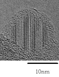 Fig. 1 HRTEM image of nanocrystalline silicon. 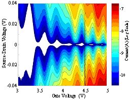 Fig. 2 Single electron tunneling characteristics in a silicon quantum dot device. 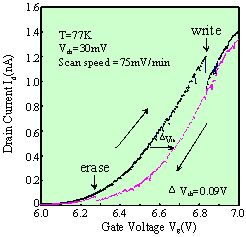 Fig. 3 Single electron memory characteristics. 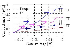 Fig. 4 Ballistic vertical transistors. |