|
|
 Semiconductor
materials and optical devices for future optoelectronic systems Semiconductor
materials and optical devices for future optoelectronic systems
T. Miyamoto Lab.
http://vcsel-www.pi.titech.ac.jp/index-e.html
Objective
The purpose of this study is to develop future optoelectronic systems
by investigation of novel semiconductor materials, quantum structures
and device structures for high performance semiconductor optical devices.
The target is new parallel lightwave systems by these optical devices.
Research Field
Optoelectronics, Semiconductor laser, semiconductor epitaxial growth
Research Theme
We are developing novel semiconductor materials for high performance
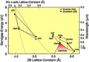
laser devices. The GaInNAs shown in Fig. 1 can be grown on GaAs and
it can emit at wavelength over 1.0 mm. It is attractive for long wavelength
vertical cavity surface emitting lasers (VCSELs) because of applicability
of matured VCSEL technologies. The GaInNAs is also expected to have
a good temperature characteristic due to its material property. The
GaInNAs is grown by metalorganic vapor phase epitaxy (MOCVD) and molecular
beam epitaxy (MBE). The lasing operations from 1.2 mm to 1.4 mm wavelengths
have been realized. High performance long wavelength VCSEL is the
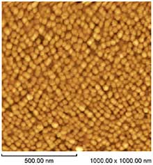
next target and GaInNAs self-organized quantum dots as shown in Fig.
2 are investigated for the future active material.
 |
 |
| Fig. 1
Bandgap vs. lattice constant of GaInNAs |
Fig.2
GaInNAs Quantum Dot
|
|
 |
|
 |