Objective
The purpose of this study is to discover the successors of today’s
VLSI technology. We investigate quantum effects in semiconductor nanostructures
and superconducting thin films.
Research Field
Quantum-effect devices, Single-electron devices, Ballistic Transistors,
Nanotechnology
Research Theme 1) Single electron devices based on plasma- derived silicon nano
crystals
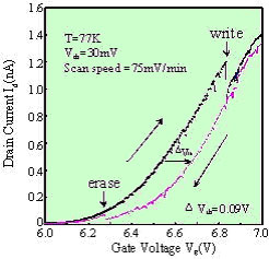
Single electron devices are promising for low-power electronics in
future VLSI and portable computer application. We are developing silicon
nanostructure devices by the self-organized formation of silicon quantum
dots using plasma processes. The advanced electron beam lithography
processes can achieve position control. Single-electron tunneling
characteristics and memory effects have been observed in silicon nano
devices at various temperatures. A new project Neo Silicon featuring
interaction between quantum dots has been launched.
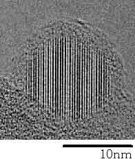
Fig 1 : HRTEM
image of nano crystalline silicon.
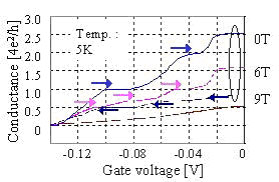
2) Silicon ballistic electron devices
Ballistic transport, electrons travel without scattering, occurs when
device size is much smaller than the electron mean free path. We have
observed clear quantized conductance, an indication of ballistic transport,
from a vertical transistor with a wrap-around gate structure. We have
also observed electron emission from nano crystalline silicon dots
with high efficiency.
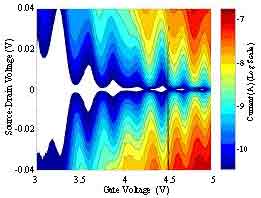
Fig 2 : Single
electron tunneling characteristics in a silicon quantum dot
device.
3) Atomic layer MOCVD of oxide ultra thin films
Very high quality superconducting and dielectric onside ultra thin
films are prepared by atomic layer MOCVD method developed in our laboratory.


 Investigation
of nanostructure quantum effect devices for future ultra-high speed
and low-power integrated systems
Investigation
of nanostructure quantum effect devices for future ultra-high speed
and low-power integrated systems