Integrated circuits by silicon changed the world. To progress further, replacement of channel material from silicon to higher mobility material is required.
InGaAs is one of the candidate as nMOS material and we studied InGaAs MOSFET.
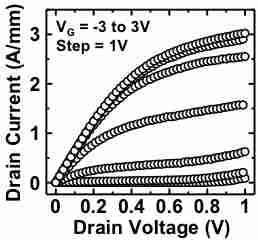
By using epitaxilally grown source, we obtained 2.4 A/mm at drain voltage of 0.5 V. To our knowledge, this is highest drain current at drain voltage of 0.5 V. Moreover,
Transistors with vertical heterostructures are attractive because of their inherent controllability of the propagation
distance of electrons. Moreover, heterostructures to obtain electron launcher or type-II junction for TFETs can be introduced by verical FETs.
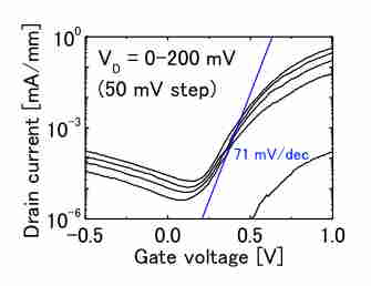
In FETs with electron launcher, transistors with channel length of 60 nm and body width of 15 nm exhibited current density of 7MA/cm2. In GaAsSb/InGaAs type-II heterojunction TFETs, SS of 71 mV/dec was confirmed.
STEM image of FETs with 15 nm-wide body
GaN HEMT is promising devices due to mirowave perfomance under suppply voltage of several tens volts and power devices. In our laboratory, normally-off operation is studied.
Compound semiconductor is promising material because of its inherent properties of higher mobility.
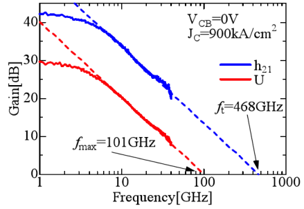
In compound semiconductors, InP related materials exhibits highest cutoff frequency over 500 Ghz.
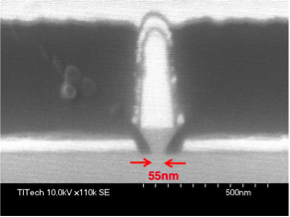
In our lab, we fabricated ultarfine heterojucntion bipolar transistors. To our knowledge, obtained 55-nm$2212wide emitter is narrowest in bipolar transistors. By using this narrow emitter, 5 MA/cm2 is obtained as current densty.
To reduce parasitic capacitance,
we used buried metal in semiconductor as a collector electrode. As a result, smallest total base-collector
capacitance (< 1fF) was observed. As a smallest emitter,we reported 0.1umx0.5um emitter area.
(At present, we suspend this research waiting progress of micro-fabrication technology. )
Electrons in materials are not only charge carriers but also potentially execute sophisticated functions
based on the quantum wave nature, for example, Fourier transformation achieved by manipulating an electron wave front.
To challenge the manipulations using man-made structures, we have carried out Young's double-slit experiment for
the hot electron wave in the semiconductor fabricating structures with 25nm-space double-slit in a InP layer buried with GaInAs.
(At present, we suspend this research waiting progress of micro-fabrication technology. )
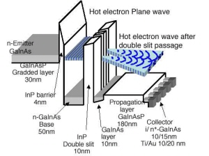
Schematic view of fabricated structure
Metal-organic vapor phase epitaxy (MOVPE) is most powerful tool to grow a compound semiconductor heterostructure at present. We started our MOVPE research in 1980 and have many experience including design for homemade MOVPE. Even at present, we continue the improvement of purity of materials and highest mobility in 2DEG struture at 77 K was reported in 2003.
To write a arbitrary pattern, electron beam lithography (EBL) is mot powerful tool and we used the lithography in many fabrication processes. But resolution limit and line edge roughness of EBL must be studied to improve the process. At present, the limitations were caused by eletron beam resist. By using our EBL machines with 4 nm as beam spot size, we have studied resolution limit and line edge roughness of EBL.