
| Research theme |
|
üĪMembrane photonic circuits |
| ü@ |
| Research |
| Membrane photonic circuits (Details) |
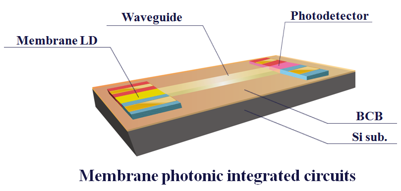 |
| ü@An introduction of photonic integrated circuits (PICs) for on-chip interconnects is considered as a promising solution to replace global electrical wiring on Si-LSIs. For this purpose we have proposed the concept of a membrane PIC composed of InP-based photonic platform with a membrane structure (high-index-contrast waveguide with the thickness of around 200 nm) bonded on Si or SOI substrate using a benzocyclobutene (BCB) adhesive wafer bonding method. The high index contrast (HIC) waveguide structure which enables ultra-small and highly integrated optical circuits is very attractive for realization of low power dissipation photonic devices. Recently, lateral current injection (LCI)lasers with thin core layers have been demonstrated as an application for current injection structure. As a results, very low threshold lasing of optically and also electrically pumped membrane DFB laser have been obtained. With these technologies, we are also engaged in membrane based photodetectors, modulators and waveguides to realize photonic integrated circuits on membrane platform. |
| üóü@To top of the pageü@üó |
| Si/III-V Hybrid integration (Details) |
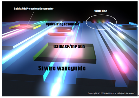 |
| In recent years, with the rapid increasing of internet traffic, researches are being done to produce large-scale Optical Integrated Circuit possessing high efficient and high capacity optical routing tool. AS an approach, to manufacture optically active devices like optical source and amplifier using III-V semiconductors on Si platform üeIII-V/Si Hybrid Integration processüf is available. Si is a transparent and low-loss medium within communication wavelength band and small-size optical circuit can be manufactured using Si, it is possible to do large-scale integration by CMOS process at low cost. As III-V group semiconductors like InP are direct-bandgap semiconductors, it is possible to realize optical devices using III-V semiconductors which will be difficult to realize using indirect-bandgap Si. In this group, we emphasize on the characteristics of each InP optical source and Si optical waveguides and use their combined structure to realize multi-function optical integrated circuit which is difficult to realize with only InP or Si. |
| üóü@Top to the pageü@üó |
| Optical intergrated circuits on LSIs (Details) |
 |
| ü@Appearances of a high-capacity and high quality media, such as 3D-movies and videos have led higher data transaction capability of LSIs. The required clock frequency and total data stream for LSI chips are expected to exceed 5 GHz and several Tera-bits/sec by 2019. For achieving the requirement, miniaturization technology of the complementary metal oxide semiconductor (CMOS) transistors can enhance the operation speed of the local wire layer. On the other hand, the signal delay in the global metallic wires, which connect between blocks in a LSI-chip, is limiting the total LSI performance due to the skin effect. As one of the long-term solutions, introduction of optical circuits on the LSIs is proposed as well as 3D-LSI chip technology. And for the optical circuits on the LSIs, silicon photonics technology have evolved drastically during the past ten years due to the superiority in the integration of electronics and photonics, which are both based on the same silicon-platform. Our research group has mainly challenged to the following two topics. |
| üóü@Top to the pageü@üó |
| Metamaterial devices (Details) |
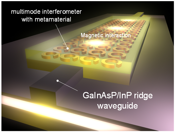 |
| ü@Optical metamaterials offer new opportunities for innovation in the field of electromagnetic parameter design, such as the design of permittivity ā├ and permeability ā╩. The major focus of attention is to create artificial materials with unique ā├-ā╩ values that cannot be observed in any existing media and to take advantage of these expanded parameters for better control of electromagnetic waves. Recent progress in optical metamaterials has allowed researchers to move material properties away from the non-magnetic line ā╩ = 1 and has opened the third quadrant of the parameter space (i.e., ā├üā0 and simultaneously ā╩üā0), which was previously inaccessible. One of the next trends is to think of metamaterials as devices, where the structuring of metal and the hybridization with functional agents brings new functionality. Especially, introducing optical metamaterials into actual photonic devices poses an exciting challenge. Much effort has been expended in the development of advanced optical applications using the concept of metamaterials. In our laboratory, we demonstrate InP-based optical devices combined with metamaterials to show the possibility of permeability control on the semiconductor-based photonics platform. |
| üóü@Top to the pageü@üó |
| ü@ |
| Transistor Laser (Details) |
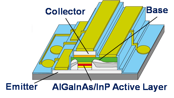 |
We propose a new light source üeüeTransistor Laser (TL)üfüf for next generation optical communication. Different from Laser Diodes (LDs), TL has 3 terminals; emitter, base, and collector. Electrons injected from an emitter are diffused, and a portion of the electrons is recombined at the active layer while the rest are removed from the collector. Due to this carrier flow, fast carrier supply to the active layer is realized and as a result, high-speed modulation beyond conventional LDs can be achieved. Now, we start demonstrating modulation with TL. |
| üóü@Top to the pageü@üó |
| Optical/THz signal converter (Details) |
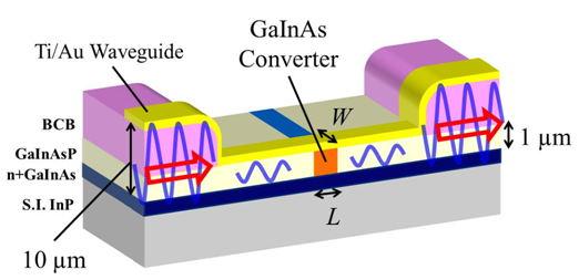 |
ü@Optical circuits and optical networks are being installed everywhere from long-haul to inter/intra chip networks due to the high capacity of their data rate. On the other hand, because of the wider bandwidth capability compared to microwaves used in conventional wireless communication systems, sub-THz and THz waves are expected to be crucial frequency-bands in next generation wireless communication systems. Therefore, it is very important to realize a direct signal conversion method between THz wave signals and optical signals. Until now, we devised a novel direct converter structure utilizing photo carrier generated gate in THz waveguide and analyzed its fundamental characteristics. |
| üóü@Top to the pageü@üó |
| Distributed reflector (DR) laser integrated with active and passive sections (Details) |
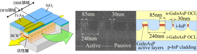 |
| ü@We propose a new method of monolithic integration by using the energy blue shift due to the lateral quantum confinement effect. Using this technique, we realize a new type of distributed reflector (DR) laser consisting of a DFB section with wirelike active regions and a distributed Bragg reflector (DBR) section with a quantum-wire structure. For low threshold and high efficiency operation, we designed the low-loss waveguide using the energy blue shift due to the lateral quantum confinement effect. As a result, the DR laser with the low-threshold, high efficiency and single-mode operation can be achieved. |
| üóü@Top to the pageü@üó |
| Quantum-wire laser (Details) |
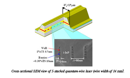 |
| ü@We realized a RT-CW operation of GaInAsP/InP quantum-wire lasers (wire width of 23 nm in a period of 80 nm, 5-stacked quantum-wires) fabricated by EB lithography, CH4/H2-reactive ion etching and 2-step OMVPE growth processes for the first time. From RT-CW lifetime measurement, no noticeable performance degradation was observed even after more than 12,000 hours. Good size distributions of multiple-quantum-wire structures have been obtained with standard deviations less than ?2 nm. ü@GaInAsP/InP quantum-wire lasers with narrow wire structures (wire width of 14 nm in a period of 80 nm, 5-stacked quantum-wires) were realized. Lateral quantum confinement effect in this quantum-wire laser could be observed via sharper shape of the EL spectrum than that of quantum-film lasers in the higher transition energy region. ü@In future, we aim to realize the narrow spectral width with good size uniformity of quantum-wires and the low threshold current operation of Q-Wire lasers by applications of distributed Bragg reflector (DBR) structure and DFB cavity. |
| üóü@Top to the pageü@üó |
| ü@ |
| Distributed feedback laser with wirelike active regions (Details) |
 |
| ü@Although DFB lasers with partially etched quantum wells have been reported from several reseach groups, excellent characteristics of DFB lasers with completely etched wirelike active regions are experimentally shown. Threshold current dependence on the laser with wirelike active regions is investigated. And also, superior lasing properties of this type of BH-DFB LD, such as submilliampere and stable single-mode operations will be given. |
| üóü@Top to the pageü@üó |
| ü@ |